BC547 » The NPN bipolar transistor clearly explained
This text is machine translated.
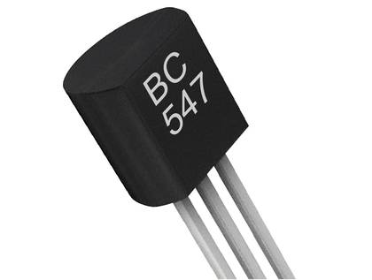
When hobby electronics engineers or electronics trainees want to build a transistor circuit, they like to use the electronic component BC547. The reason is actually quite simple.
The inexpensive NPN transistor BC547 is small but still quite handy. It has a sturdy TO-92 housing and the long connection wires make it easy to insert into circuit boards. Alternatively, it can also be freely wired for test purposes. This is very quick and you can easily make changes to the circuit or eliminate errors.
The BC547 NPN transistor also has a wide range of technical features, which means it can be used in many circuits and applications. These are sufficient reasons for us to take a closer look at the transistor. We will explain the basic functions of bipolar transistors as well as the difference between NPN and PNP.
The word transistor is made up of the two words “transfer” and “resistor”. And due to its properties, a transistor can actually behave like a variable electrical resistor or a switch.
The historical development
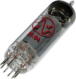
The first theoretical preliminary work on the transistor took place as early as the 1920s. The search was on for a replacement for the vulnerable electron tubes.
However, it was not yet technically possible to produce high-purity silicon or germanium. It was not until the 1940s that the germanium transistor was invented in the USA and at the same time in France.
Although the semiconductor developed in France with the name “Transitron” had lower noise values, better stability and a longer service life, the “French transistor” unfortunately failed to achieve commercial success.
Today, transistors are made of silicon and are used in electrical circuits as contactless switches, regulators, impedance converters or amplifiers. These diverse functions are possible because a transistor is able to influence a high load current with a small control current. A relay could also perform the same function, but the transistor is much faster and there are no mechanical components in a transistor. This means that a transistor is not subject to mechanical wear.
In addition to the use of individual transistors, transistor technology is also used in integrated circuits (ICs). More and more transistors are being integrated into an IC housing. The most modern and fastest processors and microcontrollers now contain several billion transistor elements.
The BC547 transistor is basically a semiconductor made of silicon, which is constructed in a similar way to a diode. We have already described the exact function of a diode with doped silicon in more detail in our technology lexicon.
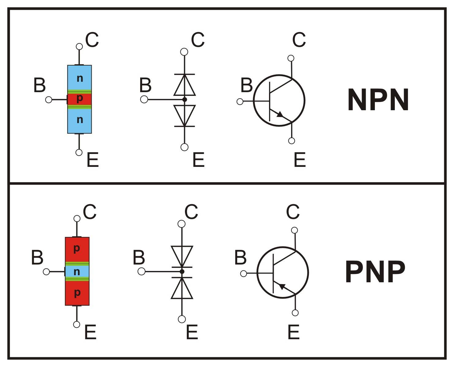
Unlike a diode, a transistor does not have just one pn junction. By stringing together differently doped semiconductors, two pn junctions are created.
This is why these transistors are also referred to as bipolar transistors, BJT transistors or simply BJT (bipolar junction transistor).
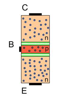
As each of the differently doped silicon semiconductor elements of the double diode requires its own connection, a transistor has three electrical connections.
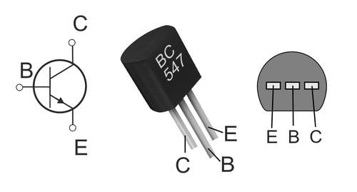
The connection of the middle semiconductor element is called the base (B). The upper connection is the collector (C) and the lower connection is called the emitter (E). In principle, the collector collects the electrons that the emitter emits.
Because of the two pn junctions, two diodes connected in opposite directions (double diode) are often used as an equivalent circuit diagram to explain the design principle of a transistor. However, it is not possible to simulate the operation of a transistor with two separate diodes. After all, one of the two diodes will always prevent the flow of current. The reason why a transistor reacts completely differently in this respect lies in its structure and in the very thin base layer. In the pictures shown, this is only shown much wider than it actually is for visual reasons and for better understanding.
Even though the collector and the emitter are made of the same doped material, there is a difference: the emitter is much more highly doped than the collector. This means that it has far more impurity atoms.
Depending on how the individual semiconductor elements are doped, there are bipolar PNP transistors and NPN transistors. The basic function of both transistor types is identical, but they differ in the direction of the current. The respective technical current directions are indicated by differently aligned arrows on the emitter connection.
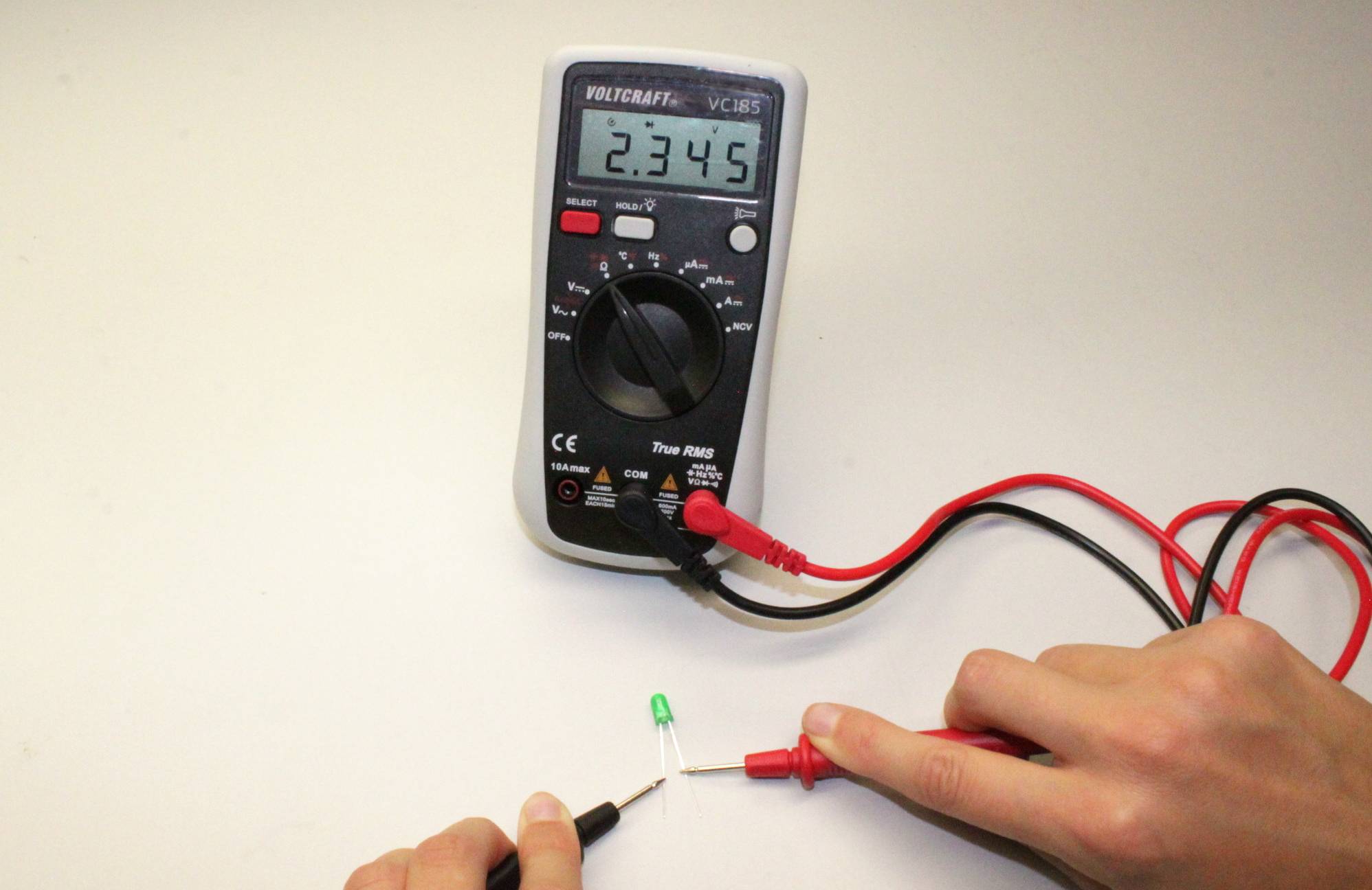
Using a multimeter with a diode tester, the diode function of the two pn junctions can be measured between the base and emitter and between the base and collector of bipolar transistors.
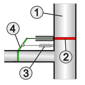
Before looking at the internal structure of a transistor, you should first familiarize yourself with its basic function. A water pipe with a water slide is ideal for this purpose.
Comparison with a water pipe slide valve
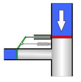
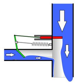
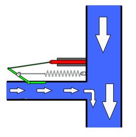
With a transistor, you can control a high current from the collector to the emitter with a low current from the base to the emitter. The specified current direction refers to the technical current direction from plus to minus.
This can be imagined as a water pipe (1) with a lateral connection and gate valve (2).
A tension spring (3) pushes the control flap (4) into the stop position. In this position, the control flap and the gate valve are closed.
Function of the semiconductor element
As the BC547 transistor is an NPN transistor, we will also explain how it works using an NPN transistor. In a PNP transistor, only the doped layers are arranged differently and the current direction is reversed. However, the basic functions are identical for both transistor types.
Important: In order to understand the function of a transistor semiconductor element correctly, you should not take the technical current direction from plus to minus as a basis. It is better to look at the physical direction of current, i.e. the flow of electrons from the negative pole of a voltage source to the positive pole of the voltage source.
The two n-doped areas at the emitter (E) and the collector (C) each have an excess of free electrons (blue dots).
The middle area of the base (B) is p-doped and has an excess of defect electrons or holes (dark dots).
As with a diode, a barrier layer is created at each of the two pn junctions by recombination, in which the free electrons fill the holes.
As the barrier layer no longer has any free electrons, it acts like an insulator.
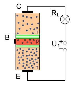
In order for electrons to flow from the emitter (E) to the collector (C) of a transistor (NPN), the two connections must be connected to a voltage source (U1). In the case of the NPN transistor BC547, the collector must be connected to the positive terminal of the voltage source and the emitter to the negative terminal. To limit the current through the transistor later, a lamp is used as a load resistor (RL).
By applying the voltage (U1), the proportion of electrons in the emitter is increased and the proportion in the collector is reduced. This also changes the junction layers. The layer between the base and emitter becomes thinner and the layer between the base and collector becomes thicker. However, the blocking effect is still so high that no current (electrons) flows across the emitter/collector path and the lamp does not light up. The transistor is blocked.
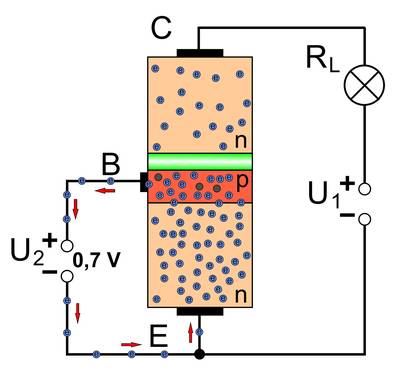
To make the transistor conductive, another voltage (U2) must be connected to the base. The base is connected to the positive terminal and the emitter to the negative terminal of the second voltage source (U2). As long as the voltage at the base is below 0.7 V, nothing happens and the transistor is still blocked.
When the voltage of the base-emitter path reaches the 0.7 V limit, the boundary layer between base and emitter is no longer effective and the electrons can flow from the n-doped area of the emitter into the p-doped area of the base.
However, only a very small proportion of the electrons are diverted via the base connection to the voltage source (U2). In addition, there are only very few holes available in the thin p-doped base layer that can accept electrons.
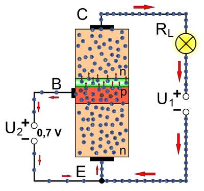
For this reason, the electrons tunnel through the boundary layer between the base and the collector. They virtually get lost in the n-layer of the collector. There they are attracted by the high positive potential of the collector and flow from the collector connection to the positive pole of the first voltage source. Electrons (electric current) therefore flow from the emitter to the collector. As this closes the circuit, the lamp also lights up.
The thinner the base layer, the stronger this current conduction effect. With a very thin base layer, the current from the emitter to the collector is many times higher than the current from the emitter to the base. In addition, the collector current reacts directly proportional to the base current. Slight changes in the base-emitter voltage and therefore the base current cause a large change in the collector current. The current fluctuations at the base are therefore amplified by the transistor.
The typical current amplification factor of the BC547C is approx. 420 - 800, which means that a current change of only 1 mA at the base causes a current change of 420 - 800 mA at the collector. Further important data can be found in the manufacturer's technical documentation if required.
In addition to the current amplification already mentioned, the BC547 transistor can also amplify the voltage. On the one hand, only a very small change in the voltage at the base is required to cause a change in the base current of just 1 mA. On the other hand, a change in the collector current of 420 - 800 mA has a very strong effect on the voltage at the collector resistor (load resistor). This is why transistors are often used as voltage amplifiers.
How high the voltage amplification or the current amplification actually is in the respective circuit depends on the basic circuit in which the transistor is operated and how the design of the external circuit was selected.
Voltage amplification in the emitter circuit
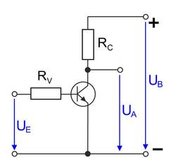
The function of voltage amplification can be nicely demonstrated using an emitter circuit. The emitter circuit is one of three possible basic circuits for operating transistors in electronic circuits. The basic transistor circuits are explained in more detail below.
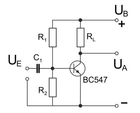
In addition to the NPN transistor BC547, three further resistors and a capacitor are installed. According to the transistor's data sheet, the operating voltage +UB can be up to 45V.
The resistors R1 and R2 are designed so that a voltage of approx. 0.6 V is set at the base. The resistor RL acts as a load resistor for the transistor and limits the current across the collector-emitter path.
The capacitor C1 serves as a coupling capacitor. It ensures that the input signal is not superimposed by the DC voltage on the transistor. Low-frequency audio signals, on the other hand, can pass through the capacitor without any problems.
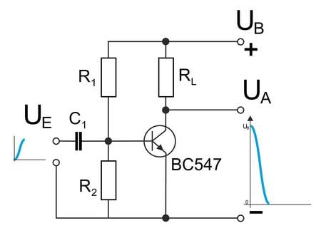
Without a control signal, the transistor blocks. As no electric current flows through the resistor RL, no voltage drops across the resistor. The operating voltage +UB is applied to the collector or output UA.
When the input signal increases, the voltage change is transferred to the base of the transistor via the capacitor. The base-emitter voltage therefore increases. From a value of 0.7 V, the base-emitter path and therefore the transistor begins to conduct. The collector-emitter path reduces its resistance value and current flows through the resistor RL and the collector-emitter path. The collector-emitter voltage or the output voltage UA begins to fall.
When the voltage at the base of the transistor is so high that the transistor is fully controlled, the output voltage has reached its minimum value. The voltage will not drop completely to 0 volts, as a small residual voltage drops across the collector-emitter path of the transistor even when it is fully switched on.
When the voltage of the input signal drops, the voltage at the output rises again. As soon as the voltage at the base falls below the 0.7 V limit and consequently no more base current flows, the voltage at the output is back at the level of the operating voltage +UB.
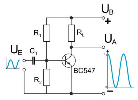
If a sinusoidal AC voltage is used for control, the AC voltage, which is amplified many times over, can be tapped at the output.
In addition to the voltage amplification already mentioned, it is also easy to see that in an emitter circuit the output signal is 180° out of phase with the input signal.
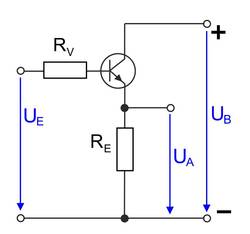
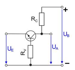
The basic transistor circuits are named after the transistor connection, which is the common reference point for the input and output signals and is connected to ground in terms of AC voltage. The respective connection does not necessarily have to be connected to earth. The transistor connection shared by the input and output signals can also be connected to the positive voltage potential. This is because the charging capacitors in the power supply unit represent a short circuit for an AC signal voltage.
Depending on which transistor connection is shared by the input and output signal, there are three different basic circuits:
Properties of the basic transistor circuits at a glance:
| Feature | Emitter circuit | Collector circuit | Basic circuit |
|---|---|---|---|
| Voltage amplification | High | Low | High |
| Current amplification | High | High | Low |
| Input resistance | Medium | High | Low |
| Output resistance | Medium | Low | High |
| Cut-off frequency | Low | Medium | High |
How is the BC547 transistor connected correctly?
For correct operation, it is important that the transistor is installed correctly in the circuit. The respective assignment of the three connection legs can be found in the technical documentation. In the case of the BC547, we have listed the pin assignment again here.
Is it possible to test the function of a transistor when it has been removed?
Yes, you can! A simple digital multimeter with a diode test function is sufficient. This can be used to check whether the two pn junctions of the double diode are OK.
The diodes between base and emitter and between base and collector must allow the test current of the measuring device to pass in one direction and block it in the other direction. The transistor between the collector and emitter must have a high impedance in both directions.
What do the letters “A”, ‘B’ or “C” after the transistor designation mean?
The letters stand for the different current amplifications. The BC547C component has almost three times the current gain of the BC547A transistor. The exact values can be found in the manufacturer's technical information or the data sheet for the respective transistors.
What does RoHS mean in the technical data?
RoHS is the abbreviation for Restriction of Hazardous Substances. The directive for the protection of human health and the environment serves to restrict hazardous substances such as lead or cadmium in electrical and electronic devices and their components.
