1N4148 Diode » Structure & function of the Si diode simply explained
This text is machine translated.
Updated: 29.07.2022 | Reading time: 8 minutes
There is probably no other diode that is as popular with circuit developers, service technicians, hobby electronics engineers and manufacturers as the 1N4148 small signal diode. It is therefore no wonder that these small and durable diodes are installed in almost every electronic circuit.
The main reason for this is the price. The universal diode is available for just a few cents. But it's not just the price, the technical performance characteristics of the diode are also impressive. Here we explain in more detail what the 1N4148 can do and how a diode works.
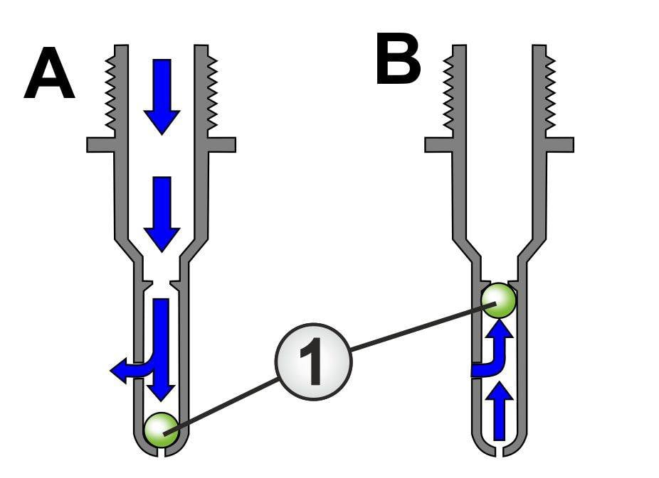
A diode is an electronic component that only allows current to flow in one direction. This is similar to a valve on a bicycle tire or car tire. With an intact valve, the air can also only flow through the valve in one direction. Whether the valve allows the air to pass through or is closed depends on which side the pressure is higher.
If you attach an air pump to a bicycle valve and generate a higher air pressure than is present inside the tire, the air flows through the valve into the tire. The valve ball (1) is pressed down by the inflowing air (sketch A).
If the tire is fully inflated, the air pressure inside the tire is higher than outside. The valve ball (1) is pressed upwards and closes the air valve (sketch B).
A diode works on the same principle, except that it conducts electricity instead of air.
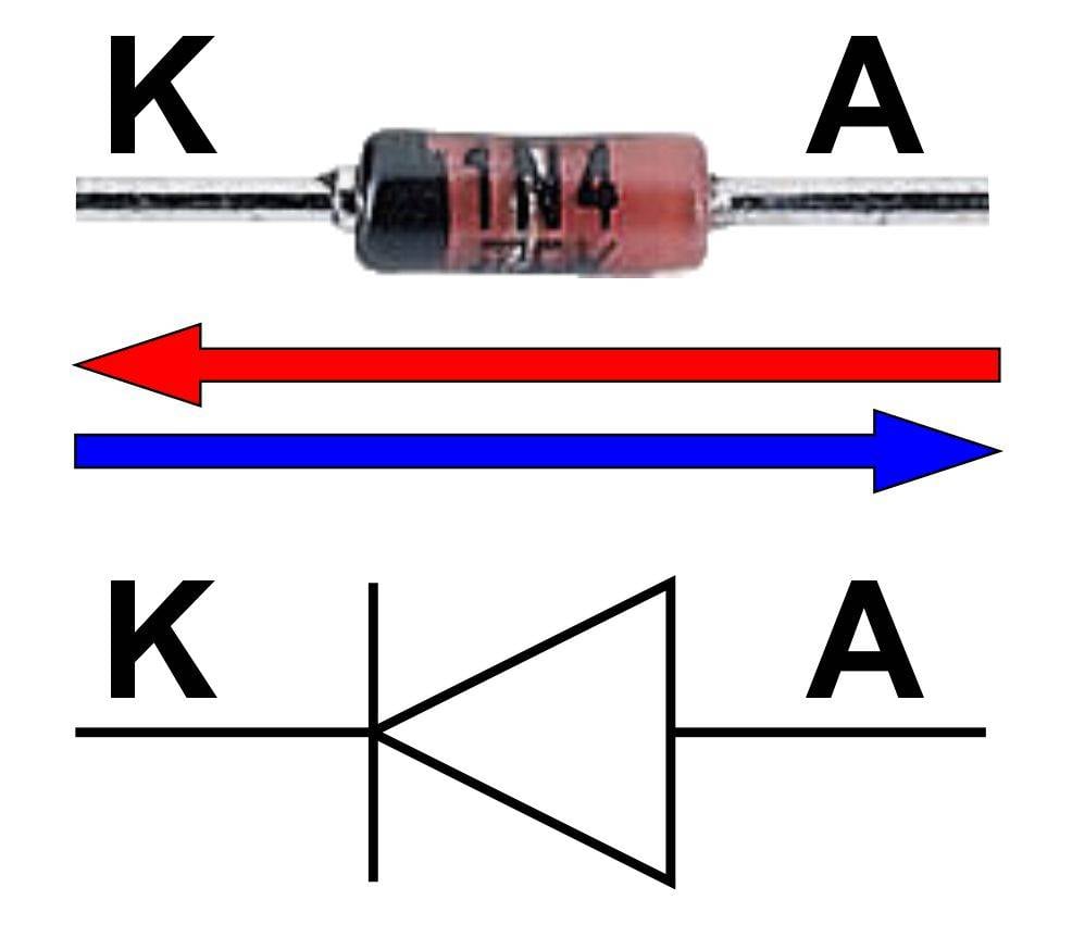
The two connections of the diode are called the anode (A) and cathode (K). If the externally applied voltage at the anode is at least 0.7 V higher than at the cathode, the diode is conducting. This means that the diode allows the current to flow from the anode to the cathode and behaves like a closed switch. This current direction is also referred to as the forward direction (red arrow).
If the voltage difference between the anode and cathode is less than 0.7 V, the diode blocks the current flow. In this case, the switch is open. If the polarity of the voltage is reversed and the higher voltage potential is applied to the cathode, the diode also blocks. The blocking direction (blue arrow) therefore runs in the opposite direction to the forward direction - i.e. from the cathode to the anode.
How high the respective values for the forward current and the reverse voltage may be depends on the diode type and the manufacturer. The exact values can be found in the manufacturer's information and data sheets.
In order for a diode to conduct or block the current under the specified conditions and thus work as a switching diode, a semiconductor element must be used. This is why diodes are considered electronic components.
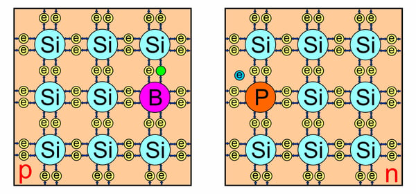
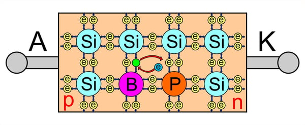
A semiconductor is a material that has the properties of conductors and insulators. In the case of the 1N4148 diode, the semiconductor element consists of pure silicon, which has four electrons on the outer shell (valence shell). However, as the outer shell has space for up to 8 electrons, a silicon atom can form an atomic bond with up to four other silicon atoms. This means that there are eight electrons on the valence shell. During doping, foreign atoms are incorporated into the lattice structure of the silicon. The foreign atoms must be designed in such a way that they fit well into the lattice structure of the silicon.
If the silicon (Si) is p-doped, boron atoms (B) or aluminum atoms, for example, are inserted. In contrast to silicon, both atoms only have 3 electrons (e) on the outer shell. The free space that could accommodate a fourth electron is referred to as a “hole” or “defect electron”. If a neighboring electron jumps into the free space, the hole virtually moves through the silicon crystal.
If the silicon is n-doped, phosphorus atoms (P), for example, are inserted. In contrast to silicon, the phosphorus atoms have 5 electrons on the outer shell. This means that there is always one electron left per phosphorus atom, which can also move freely through the silicon lattice structure.
What happens at a pn junction?
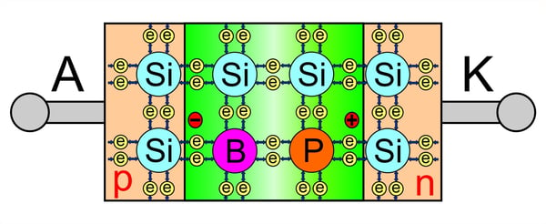
If an n-doped and a p-doped silicon crystal are now joined together, diffusion takes place.
The holes in the p-doped part, which represent a lack of electrons, move to the right to the n-doped part with the excess electrons.
And the electrons from the n-doped part move to the left to the holes in the p-doped part with the electron deficiency.
The migration of the electrons, which in principle represent negative charge carriers, creates an internal electric field at the boundary layer between the two differently doped areas (see green area in the figure).
As there are now more electrons in the p-doped area than before due to diffusion, a negative pole is created here. In the n-doped area, the migration of the negatively charged electrons creates a positive pole.
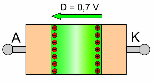
The effect of the resulting electric field (see green arrow) slows down diffusion. This is because the negative pole of the electric field prevents further electrons from moving into the p-doped area. The positive pole ensures that no further holes move into the n-doped area.
Diffusion is complete when the electric field is so strong that no further unions of free electrons with the existing holes take place.
For silicon diodes, the diffusion voltage (D) of the internal electric field is 0.7 V. For germanium diodes, the value is approx. 0.3 V. As there are no free electrons in the area of the electric field, this area does not conduct current. This is why this layer is also called the barrier layer.
Important: The build-up of the barrier layer is completely automatic, without any external influence on the pn junction. In order to illustrate the function of the junction visually, the junction is shown disproportionately large in the attached images. Depending on the type of diode and dielectric strength, the actual thickness of the layer is in the µm range. In other words, only a fraction of a millimeter.
As already mentioned, a diode can be operated in two directions. In the forward direction, it should allow the current to pass through as an electrical conductor. In the reverse direction, it acts as an insulator to prevent the flow of current.
Operation in the direction of passage
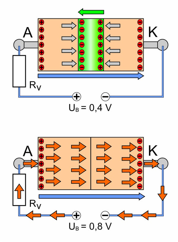
When operating in the forward direction, the voltage at the anode is higher than at the cathode. A voltage with an external electric field (see blue arrow) builds up across the diode.
This external electric field is polarized in the opposite direction to the internal electric field of the junction and effectively counteracts it. As a result, the external electric field can influence the internal field.
If the external voltage (UB) is 0.4 V, for example, the internal electric field is weakened and the junction becomes correspondingly narrower. However, the voltage of 0.4 V is not yet sufficient for the diode to conduct.
Only when the external voltage (UB) exceeds the 0.7 V limit and is 0.8 V, for example, is the external electric field stronger than the internal electric field and the barrier layer is no longer effective.
The diode now acts as a conductor and allows the current to flow. However, the voltage drop in the direction of flow is 0.7 V. This voltage drop is independent of the current. The remaining differential voltage to UB of 0.1 V drops across the series resistor Rv in the example shown.
If the external voltage falls below 0.7 V again, the junction in the diode builds up again automatically and the diode blocks the current flow.
Operation in blocking direction
When operating in the reverse direction, the voltage at the cathode is higher than at the anode. A voltage with an electric field builds up again across the diode.
However, in this case the external electric field has the same polarity as the internal electric field of the junction.
As a result, the inner field is strengthened and the insulating barrier layer is widened.
In this case, the diode will not allow any current to flow. Although a reverse current is specified in the technical data in most cases, it is so minimal that it is negligible.
As already mentioned, a diode can be used as a conductor or as an insulator. However, the current that the diode can conduct and the voltage that is blocked by the diode are limited. The values depend on the physical structure and the temperature of the semiconductor.
In the case of the 1N4148, the maximum continuous current is approx. 300 mA, although the diode can also withstand a short-term current peak of 500 mA.
The maximum reverse voltage is 75 V, whereby the diode can also withstand a short-term voltage peak of 100 V.
The maximum power dissipation of the 1N4148 diode is 500 mW at 25 °C.
The specified values vary slightly from manufacturer to manufacturer and may not seem very high at first. However, when you consider that the diode is housed in a small glass casing measuring only approx. 2 x 4 mm, the values are put into perspective. This means that the diode requires very little space in the circuits and the glass body makes the diode insensitive to mechanical stress.
Another important criterion is the switching frequency, i.e. how quickly the diode can switch from the conducting to the blocking state and back again.
The 1N4148 scores highly in this area. Because the pn junction has an extremely low internal capacitance, switching from the conducting to the blocking state takes place in just a few nanoseconds. This means that a 1N4148 diode can be used for frequencies of 100 MHz (100 million oscillations per second).
If you also consider the low price, it becomes clear why the 1N4148 diode is so popular with circuit designers and developers.
The 1N4148 switching diode has many areas of application. In addition to general switching tasks, e.g. in logic circuits or in consumer electronics devices, the diode is also ideal for extremely fast switching tasks. The 1N4148 is also ideal for protective circuits in signal processing or for high-speed rectification.
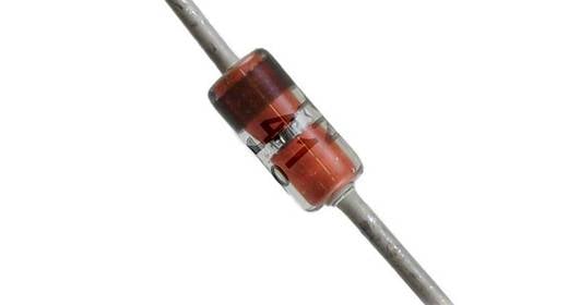
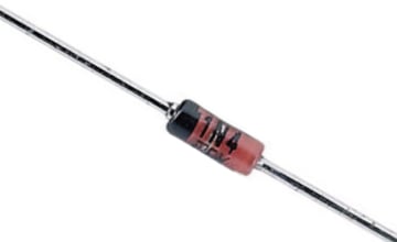
To ensure that the diode is inserted correctly into the circuit, the cathode on the glass body is marked with a ring.
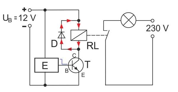
The exact function within a circuit can be explained very well if you consider the function of the 1N4148 as a freewheeling diode.
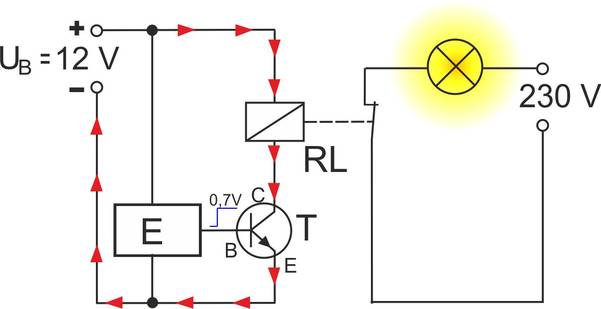
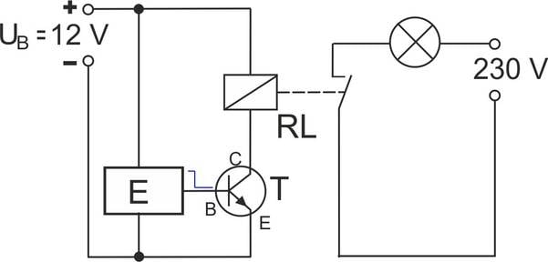
DC relays (RL) are very often used in electronics to switch large loads with a low control voltage. In the example shown, a relay with a 12 V operating voltage (UB) is used to switch a powerful 230 V lamp (L). The relay itself is switched via a small transistor (T), which in turn is controlled by electronics (E). The control electronics could be a radio receiver, for example.
Switched on state
The transistor only acts as a switch. When it is activated with a positive voltage at the base (min. 0.7 V, as the base/emitter path of the transistor is also a pn junction), it closes the relay circuit.
As soon as current flows through the coil in the relay, it builds up a magnetic field. The magnetic effect attracts a small metal lever from the iron core in the coil. This lever is mechanically connected to the normally open contact of the relay. The relay then closes its normally open contact and the lamp lights up.
Switched off state
If the control voltage at the base falls below 0.7 V again, the transistor blocks.
The relay is now no longer connected to the negative potential of the operating voltage and the magnetic field of the coil collapses.
The normally open contact is automatically opened by a return spring in the relay and the lamp goes out.
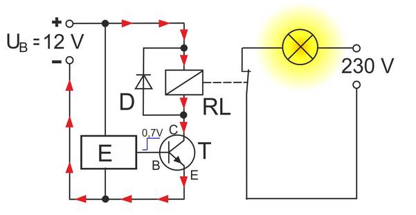
Use of a freewheeling diode
So far so simple. But there is a catch. The coil of the relay is also known as an inductor. And inductors can generate voltages when a magnetic field changes in their vicinity. This technical peculiarity is used in transformers.
And this is exactly what happens with the relay in the example circuit. As soon as the transistor blocks, there is suddenly no more voltage at the coil. Because there is no power supply, the coil's magnetic field collapses. The collapsing magnetic field in turn generates a voltage pulse in the coil. However, the polarity of this self-induced pulse voltage is reversed in relation to the original operating voltage. The positive potential is now at the bottom connection and the negative potential at the top connection.
A freewheeling diode is used so that the positive pulse of the induction voltage cannot cause any damage to the switching transistor.
Can the 1N4148 diode also be used as a mains rectifier?
The diode is not suitable as a rectifier for the 230 V AC voltage, as the dielectric strength is not given. After all, the 1N4148 is a small signal diode. Diodes of type 1N4007 would be more suitable for mains rectification, as they have a higher dielectric strength in the reverse direction.
In which designs is the 1N4148 diode supplied?
In addition to the wired version, the diodes are also available in SMD and MELF designs.
What does the ring on the housing of a wired diode mean?
The ring on the housing marks the cathode so that the diode can be inserted correctly into the circuit.
