CD 4060 Binary counter » Structure and function of the logic IC clearly explained
This text is machine translated.
Published: 14.03.2023 | Reading Time: 8 minutes
Switching tasks that control certain time sequences very often have to be implemented in electronics. However, this does not necessarily require the use of a digital clock.
A few components are often sufficient, which then generate an alternating voltage with a certain frequency as an oscillation stage. However, a continuous series of oscillations cannot be used to control a timed switching task. Instead, the individual pulses of the oscillation frequency must be counted and a switching operation carried out after a certain number of pulses.
As a 14-stage binary counter, an IC with the ID 4060 is perfectly suited for this and similar tasks. We would be happy to tell you more about this practical component.
In contrast to decimal counting, which uses the numbers 0 - 9, binary counting only uses the numbers 0 and 1. These can easily be represented with different voltage levels, such as 5 volts for high (H) or active and 0 volts for low (L) or passive. This is why computers use binary codes for their computing tasks.
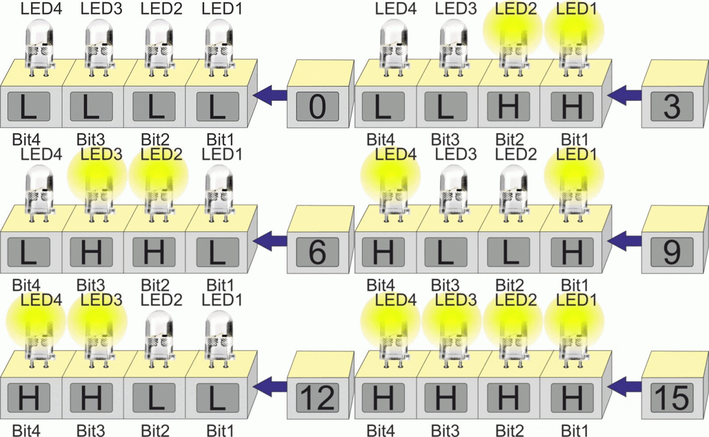
LEDs are ideally suited as bit indicators for displaying the binary states low or high, or on or off. Two binary states or the numbers 0 or 1 can be displayed with one LED (one bit). If the LED is dark, this corresponds to the value zero. If the LED is lit, this corresponds to the value one. If a further LED is added, two further on/off states can be displayed, thus extending the range of binary decimal numbers that can be displayed to 4 (0 - 3). With three LEDs, the number range doubles and eight different states (decimal 0 - 7) can be displayed.
The range of decimal values that can be displayed doubles with each additional LED. With 8 LEDs or 8 bits, 256 different decimal values can be displayed.
The attached animated image uses four LEDs to show the different lighting sequences or the sequence of high/low states that result for decimal values from 0 - 15.
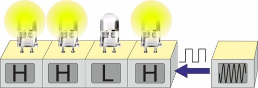
Next, an oscillator, i.e. an oscillation stage, is inserted in place of the decimal number block shown in the picture. If the oscillator is switched off, no LED lights up. As soon as the oscillator has been started and has generated the first oscillation, the first LED will light up.
Each further oscillation corresponds to the previously displayed increase in the decimal number and is displayed accordingly by the LEDs. In this case, the LEDs work as a binary counter display. This function, i.e. a switchable oscillator or generator, as well as the respective high and low outputs for connecting external LEDs or components, is performed by the CD4060 binary counter.
The 14-stage binary counter CD4060 is available with a 16-pin DIP-16 housing or as an SMD component in an SOIC-16 housing. Depending on the manufacturer, other designations such as NTE4060, MC14060 (see cover picture), HCF4060, TC4060 or HEF4060 are used for the integrated circuit (IC for integrated circuit).
Although the basic functions and the pin assignments are identical, the operating parameters, such as the maximum permissible operating voltage or the labels on the outputs, may vary slightly according to the description in the data sheet.
In order for the integrated circuit to function, the circuit first requires an operating voltage. The operating voltage is applied to pin 16 (+) and pin 8 (-) and can be between 3 and 15 V, depending on the manufacturer.
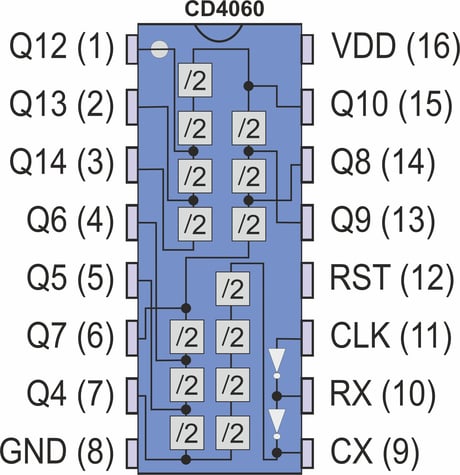
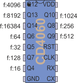
The binary outputs of the counter are routed to the outside on pins 1 - 7 and 13 - 15. Pins 9 - 11 are used to connect the internal oscillator.
Pin 12 is a reset input which switches all the IC's outputs to an L level when a high level is applied.
The exact function of the outputs and the connections of the oscillator are described in more detail in the following section.
In order to understand the function of the CD4060, you should first take a closer look at the integrated functional units.
Oscillator stage
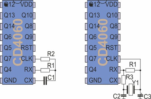
In order for the oscillator integrated in the IC to oscillate, it must be connected externally with a capacitor and a resistor. The value of the resistor R1 and the capacitance of the capacitor C1 determine the oscillation frequency or the clock for the switching at the outputs. Depending on the IC type, this can be up to 15 MHz, i.e. 15 million oscillations per second. The ceramic capacitor C1 is connected to pin 9 (CX) and the resistor R1 is connected to pin 10 (RX).
The common connection point of the oscillator capacitor and the oscillator resistor is connected to the oscillator input or clock input pin 11 (CLK) via a further resistor R2. Important: The ohmic value of resistor R2 must be significantly higher than that of R1 for the oscillator circuit consisting of R1 and C1 to function.
Even if the oscillation frequency always varies slightly due to the tolerances of the external components and temperature fluctuations, it is perfectly adequate for most circuits. If you need an absolutely stable oscillation frequency for your circuit design, you can also use a quartz Y1 (classic clock quartz with 32.768 kHz) and, if necessary, a trimming capacitor C3 instead of the capacitor C1.
Flip-flop steps
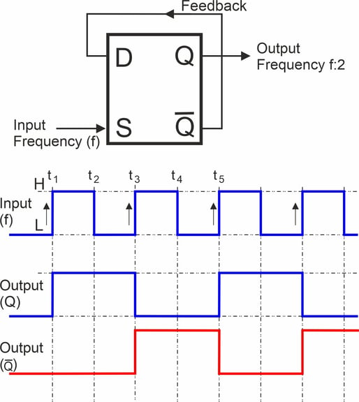
In addition to the oscillator, the CD4060 also contains a total of 14 flip-flop stages, which are connected as inverters. A flip-flop is a small electrical circuit that can assume two stable states. As long as an operating voltage is applied, a flip-flop always retains its current stable state and can be regarded as a 1-bit memory. In inverter mode, the negated or inverted output (Q with the line above it) is fed back to input D as feedback. This results in the following switching sequences:
When the operating voltage is switched on, both outputs are set to low (L). There is therefore no voltage present.
If the voltage at input S changes from low (L) to high (H), for example from 0 V to 5 V (time t1), output Q also changes from L to H. The inverted output and the associated input D remain at L. This switching state does not change. The inverted output and the associated input D remain at L. Nothing changes in this switching state, even if the voltage at input S changes back to L (t2).
Only when the voltage at input S changes to H again (t3) does the level at output Q change to L. The inverted output changes from L to H. In this case too, nothing changes at the output when the level at input S drops from H to low again (t4). The switching sequence starts again from the beginning at the next H level of the input signal (t5).
On closer inspection, it is noticeable that two high and two low levels at the input (t1 - t5) only generate one high and one low level at the two outputs. This means that the inverter flip-flop works as a frequency divider that halves the frequency of the input signal at the output.
Asynchronous counter (ripple carry counter)
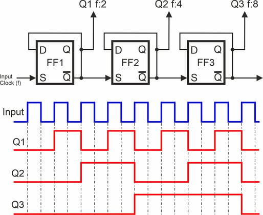
The CD4060 binary ripple counter has a total of 14 integrated flip-flop stages, which are linked in toggle mode. This means that the first flip-flop is controlled by the clock pulse of the oscillator. The inverted output (Q with dash) then controls the second flip-flop stage.
The inverted output of the second flip-flop stage then controls the third flip-flop. The sequence continues in this way. After each flip-flop stage, the frequency is halved. As a result, it takes longer and longer from flip-flop to flip-flop until the level at the output changes from L to H for the first time.
In the attached picture you can see the time-shifted voltage jumps and the frequency division at the outputs of the first three flip-flops.
Note:
The CD4060 chip only has a 16-pin DIP-16 or SOIC-16 housing. As further connections are required for the internal oscillator and the reset input in addition to the operating voltage, it is not possible with the integrated circuit to lead all outputs from Q1 to Q14 to the outside with their own pin.
For this reason, the chip designers have decided not to lead the counter outputs Q1, Q2, Q3 and Q11 to the outside.
We have also specified the division ratio to the oscillator frequency for the externally routed connections.
The easiest way to demonstrate the correct connection of the binary counter is to use a timer circuit. As already mentioned, it takes longer and longer from Q4 to Q14 until the respective output changes to the high level for the first time. This function makes it very easy to create timed circuits, such as a staircase light. Although there are special timer ICs, such as the NE555 already presented here, capacitors with a high capacity are required for very long switching times, which then have a large design and take up a lot of space. Binary counters are much more space-saving and the price is also quite reasonable.
Staircase light switch
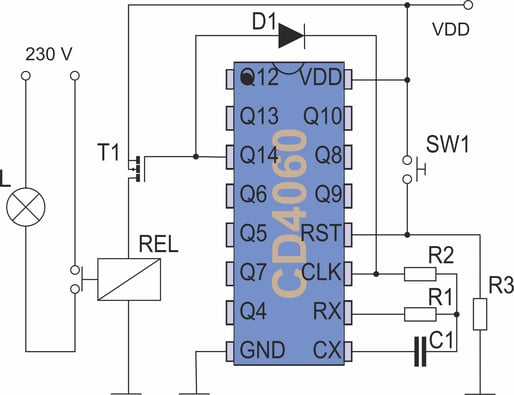
When the operating voltage is switched on, all outputs of the counter IC are initially switched to L. As the gate voltage at the P-channel FET transistor (T1) is lower than the source voltage in this case, the transistor conducts. This means that the path between the source and drain is low impedance. This allows the relay (REL) to close the switching contact and the lamp L lights up.
As soon as the output Q14 changes to high after some time, the transistor blocks and the relay drops out again, causing the light to go out.
At the same time, the high level of Q14 is switched to oscillator input pin 11 via diode D1. As a result, the oscillator frequency is no longer available. The circuit remains in this state indefinitely, as the reset input pin 12 of the binary counter is permanently connected to ground with R3.
However, if the SW1 button is pressed briefly, the reset input receives a high level and thus sets all outputs of the IC back to low. The transistor switches the light back on via the relay. It then lights up until output Q14 switches back to high.
The light duration of the lamp can be defined by the components C1 and R1. With the combination of 100 nF and 10 kOhm, the lighting time is approx. 18 seconds. The switching times can be extended by increasing the resistance and capacitance values.
In addition to its use as a frequency divider or timer, the CD4060 binary counter can also be used in other ways. We found a good example of this on the Elektor magazine website. As the circuit is both simple and ingenious, we would like to take a closer look at it.
Circuit design
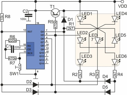
As six different states (possible cube display 1 - 6) must be displayed for a cube, three binary counter outputs (see table below) are required.
The oscillator stage consists of an RC combination (R6 and C1), whereby the oscillation frequency is fed to the input on pin 11 via R7. However, this only happens when button SW1 (with NC contact) is pressed and the oscillator input is no longer connected to ground.
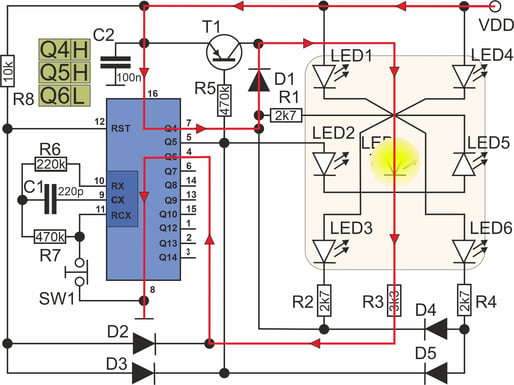
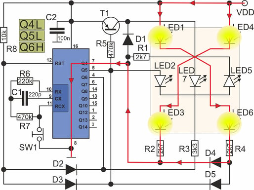
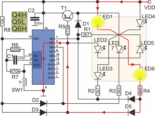
Outputs pin 7 (Q4), pin 5 (Q5) and pin 4 (Q6) are used to control the LEDs. LEDs 1 - 7 must be arranged according to the cube display. Pay attention to the current direction and polarity of the LEDs. The resistors R1 - R4 only serve as LED series resistors to limit the current.
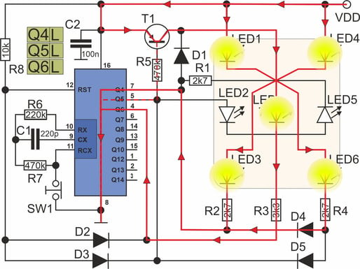
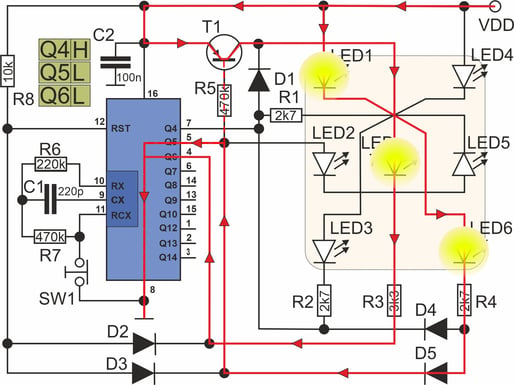
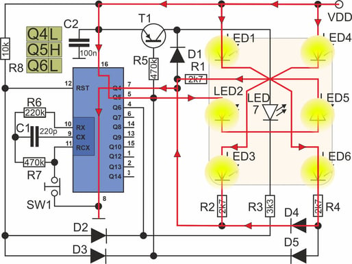
The diodes D1 to D5 (1N4148) serve as blocking diodes for the different current paths. The PNP transistor T1 with its base resistor R5 supplies power to LED7 in cube displays 3 and 5. In display 1, LED7 is supplied with power via diode D1. In order to understand the different current paths, the respective high and low levels at the outputs must be examined more closely. For a better understanding, we have first listed all eight possible switching states once again. We have structured the table according to the counting method of the couter explained at the beginning.
| Table row | Pin 4 (Q6) | Pin 5 (Q5) | Pin 7 (Q4) | Cube display |
|---|---|---|---|---|
| 1 | L | L | L | 5 |
| 2 | L | L | H | 3 |
| 3 | L | H | L | 6 |
| 4 | L | H | H | 1 |
| 5 | H | L | L | 4 |
| 6 | H | L | H | 2 |
| 7 | H | H | L | No display |
| 8 | H | H | H | Not called |
Contrary to general expectations, the display of the “number rolled” does not start with a one and the sequence of the dice display is also not consecutive. This is due to the circuitry, but does not affect the functionality.
It is much more important that the cycle starts again from the beginning after dice display 2. To do this, the counter must be reset. For this purpose, the reset input is connected to the supply voltage via resistor R8. The anodes of the two diodes D2 and D3 are also connected to the reset input. The cathodes of the diodes lead on to the outputs on pin 4 and pin 5.
Looking at the table, you can see that for every possible cube display, the outputs on pin 4 and pin 5 either alternate or have a low level at the same time. This means that the reset input is kept at a low level from the start of the counting process. The counter therefore continues to run continuously and all six dice numbers are displayed. Only when pin 4 and pin 5 in table line 7 show an H level at the same time does the voltage at the reset input increase briefly and the counter immediately starts again at line 1.
The different levels at the three outputs result in different current paths, which we have shown in more detail below.
Functional description
When the battery is connected, all outputs of the binary counter are switched to L. According to the table above, a five is displayed on the cube. This display does not change as the oscillator input is connected to earth via the SW1 button.
If the button is pressed, the signal from the oscillator is applied to pin 11 and the divider (binary divider) in the binary counter can operate. According to the table above, the binary counter now changes the cube display in an endless loop. However, the oscillator frequency is so high that switching the display is not visible to the naked eye. Instead, all seven LEDs light up continuously.
When the button is released, pin 11 is connected to earth again via the button contact and the binary counter stops. The last cube number reached during the fast cycle is now permanently displayed.
In the attached example video, we have simply connected another capacitor in parallel to C1 for test purposes and thus increased the capacitance by 200 nF. This makes the oscillator significantly slower and you can clearly see the switching between the individual displays of the cube. However, this slow version of the electronic cube is completely unsuitable for playing “Mensch ärgere Dich nicht”. After all, it is now child's play to roll any number you want.
