LM358 circuits » Structure and function of the dual operational amplifier explained simply
Updated: June 15, 2022 | Reading time: 8 minutes
This text is machine translated.
The LM358 integrated circuit is a very popular component that belongs to the category of operational amplifiers. Years ago, operational amplifiers were used in analog computers for various arithmetic operations such as addition, subtraction, multiplication, and division. But their possible applications are much more diverse. We will show you how the LM358 circuit is constructed and what possibilities this versatile component offers.
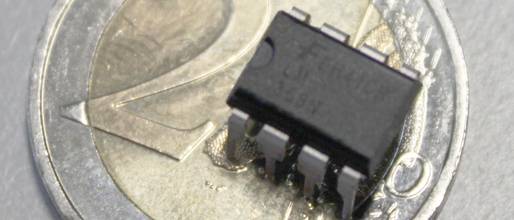
The LM358 is an integrated circuit, also known simply as an IC (integrated circuit).
An IC contains several electronic components, such as transistors and diodes, housed in a single package.
Thanks to this compact design, ICs can perform extensive and complex tasks despite their small size.
The inner workings of the LM358
When you look closely, the inner workings of an LM358 are quite straightforward. This is because there are only two operational amplifiers in a shared housing. This is why the component is also referred to as a dual operational amplifier in English.
Apart from the operating voltage, which is applied internally to both operational amplifiers, the two amplifiers operate completely independently of each other.
This means that the two inputs and the output of each amplifier are not connected and are routed out separately.
As a result, it is also possible to use only one of the two amplifiers. In this case, the connections of the second operational amplifier are not used. However, to avoid uncontrolled oscillations, circuit developers do not leave the pins open. They connect the free connections to a potential (e.g., ground). If both operational amplifiers of the IC are used for a circuit, the external circuitry must be set up accordingly.
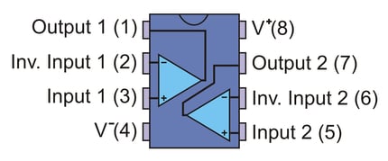
Pin assignment of the LM358 according to the data sheet
Pin 1 = Output of the first operational amplifier (Output 1)
Pin 2 = Inverted input of the first operational amplifier (Inv. Input 1)
Pin 3 = Non-inverted input of the first operational amplifier (Input 1)
Pin 4 = Negative potential of the supply voltage (V-)
Pin 5 = Non-inverted input of the 2nd operational amplifier (Input 2)
Pin 6 = Inverted input of the 2nd operational amplifier (Inv. Input 2)
Pin 7 = Output of the 2nd operational amplifier (Output 2)
Pin 8 = Positive potential of the supply voltage (V+)
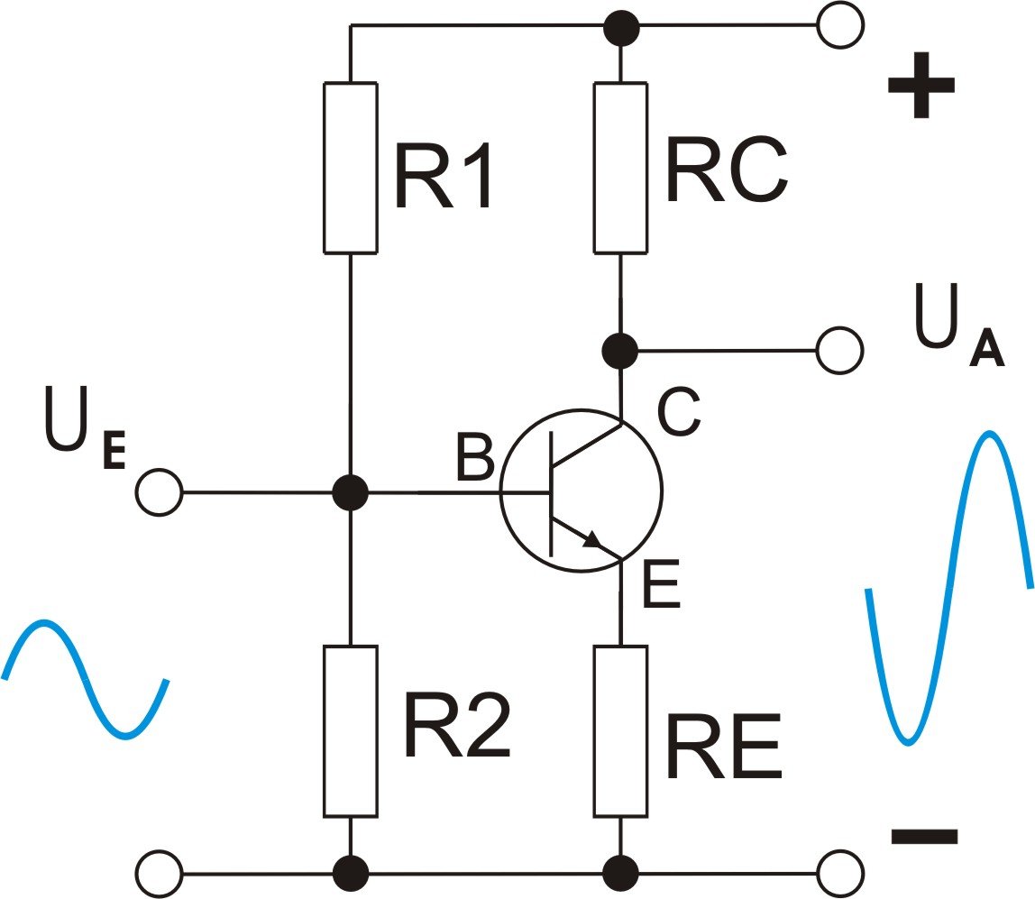
A classic signal amplifier, which is constructed with a transistor, for example, has one input and one output. In most cases, the input signal refers to the negative potential of the supply voltage, which is usually referred to as ground.
Due to its external circuitry, the transistor is designed in such a way that a small voltage change at the input causes a large voltage change at the output.
If the voltage at the input (UE) or at the base of the transistor (B) increases, the internal resistance between the collector (C) and emitter (E) decreases. The voltage at the collector therefore becomes lower.
If the voltage at the input decreases, the resistance between the collector (C) and emitter (E) increases again. The voltage at the collector rises again.
Note:
This amplifies a weak input signal with a low amplitude by a multiple of its value. However, in the transistor circuit shown, the input signal is reversed (inverted). An increase in voltage at the input causes a decrease in voltage at the output. The output signal is phase-shifted or shifted by 180°.
An operational amplifier (OPV) or operation amplifier (OP AMP) has two inputs, whereby only the voltage difference between the two inputs is amplified.
The two inputs are marked with plus (+) and minus (-). A signal at the plus input is reproduced at the output with the same phase. A signal at the minus input is output inverted, as in the transistor circuit shown above. This is why we refer to inverted and non-inverted inputs.
If the potential of both inputs changes simultaneously and in the same direction, this has no effect on the output.
Structure
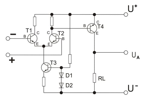
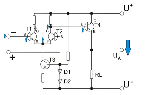
The function of an operational amplifier can be easily understood using a simplified replica with transistors.
The two NPN transistors T1 and T2 are the input transistors.
The two inputs of the operational amplifier are identical, as they are each connected to the base (B) of transistors T1 and T2. The input at which the output signal is emitted in phase is marked with a plus (+).
The input at which the output signal is rotated or phase-shifted by 180° is marked with a minus (–).
Transistor T3, together with diodes D1 and D2, acts as a constant current source or current limiter for transistors T1 and T2.
Transistor T4 is used for signal amplification. The output signal (UA) is tapped at the load resistor (RL) of T4.
Functionality
When the voltage at the non-inverted input (+) rises, the collector/emitter path (C/E) of transistor T2 becomes more low-impedance.
This causes the voltage at the collector (C) of T2 to drop and the voltage at the emitter to rise.
Since the base of transistor T4 is directly connected to the collector of T2, the voltage there also drops.
The result: The collector/emitter path (C/E) of the PNP transistor T4 becomes more low-impedance and more current flows through the load resistor RL.
The voltage drop across the load resistor increases accordingly and can be tapped at the output (UA).
Conclusion:
A positive voltage increase at the non-inverted input (+) therefore results in a positive voltage increase at the output.
When the voltage at the inverted input (-) rises, the collector/emitter path (C/E) of transistor T1 becomes more low-impedance.
This causes the voltage at the collector (C) of transistor T1 to drop.
At the same time, the voltage at the emitter of transistor T1 rises. Since the emitters of transistors T1 and T2 are connected, the voltage at the emitter of transistor T2 also rises.
This reduces the voltage difference between the base and emitter of transistor T2. As a result, the collector/emitter path (C/E) of transistor T2 becomes more high-impedance. The voltage at the collector T2 increases.
At the same time, the voltage at the base of T4 increases. The transistor now becomes more high-impedance and less current flows through the resistor RL. As a result, the voltage at RL also decreases.
Conclusion:
A positive voltage increase at the inverted input (-) therefore results in a voltage decrease or a negative voltage change at the output. The output signal behaves inversely (inverted) to the input signal.
Amplification factor
Due to its internal structure, an OPV has a very high gain factor. With a gain factor of 100,000 and an operating voltage of ±10 V, a voltage change of ±100 µV at the input is sufficient for the output to switch to either +10 V or -10 V.
For this reason, OPVs are also ideal as signal amplifiers for sensors. However, operational amplifiers can also be used as amplifiers for low-frequency and high-frequency signals or as controllers. Of course, the operating voltage sets limits on the amplification, as the output voltage cannot be higher than the operating voltage.
Impedance
In addition to the high gain factor, impedance is also of crucial importance. Since both inputs have extremely high impedance, OPVs can also be used in electrically sensitive circuits. The high internal resistance means that the signal at the input is not loaded and therefore not distorted.
On the other hand, the output signal has very low impedance and can be used directly to drive LEDs or other evaluation electronics.
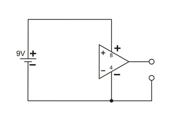
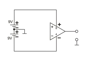
The LM358 integrated circuit has a wide voltage supply range. According to the manufacturer's data sheet, it can be supplied in two different ways:
In order to develop a basic understanding of how an OPV works and functions, we should first take a closer look at a few basic circuits.
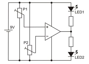
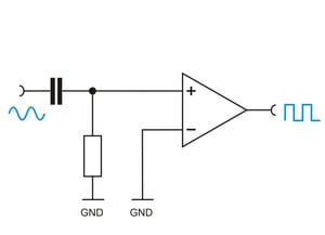
Comparator circuits
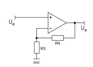
Amplifier circuit / Schmitt trigger
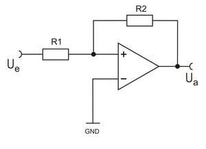
Operational amplifiers can also be used to amplify signals or to precisely determine switching thresholds. This is achieved using feedback. With feedback, part of the output signal is fed back to the input. Depending on which input the output signal is fed back to, an OPV is referred to as having negative feedback or positive feedback.
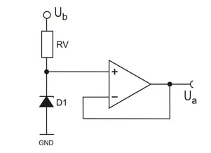
Voltage follower / impedance converter
The basic circuit of an amplifier with negative feedback is also used as a voltage follower or impedance converter.
The resistor R3 is considered to be infinitely large, i.e., virtually non-existent. The resistor R4 is considered to be a short circuit.
In this case, the gain factor is 1. The input voltage is therefore output 1:1 at the output. However, in this case, it is not about the gain, but about the high input resistance of the OPV.
In this configuration, for example, the voltage of a Zener diode can be tapped without affecting the current flow through the resistor RV and the Zener diode D1.
The voltage output by the operational amplifier corresponds exactly to the voltage across the Zener diode and can be easily loaded by subsequent evaluation or measurement circuits.
Oscillators
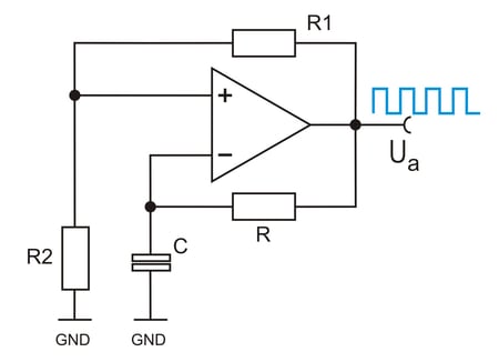
Only a few components are needed to build a simple oscillator circuit with an operational amplifier. The operational amplifier acts as a comparator that evaluates the voltage differences at the two inputs. Since even minimal voltage differences would be sufficient to trigger switching, the switching thresholds must be specifically modified.
This is done with the help of a voltage divider, which uses resistors R1 and R2 to feed part of the output signal back to the non-inverted input. This configures the OPV as a Schmitt trigger, in which the switch-on and switch-off thresholds do not coincide. The offset between the two switching thresholds is referred to as hysteresis. A capacitor (C) is connected to ground at the inverted input. The capacitor is charged or discharged via a resistor (R) connected to the output.
Information on how it works:
When switched on, the capacitor (C) is discharged and the output of the op-amp is connected to the positive voltage potential. The capacitor is now charged via the resistor (R).
As soon as the voltage at the inverted input is equal to or greater than that at the non-inverted input, the op-amp switches the output to the negative voltage potential. The capacitor is now discharged via the resistor.
If the voltage at the capacitor falls below a certain value, the circuit flips again and the operational amplifier switches the positive voltage potential back to the output. The capacitor is now charged again and the cycle begins anew.
Oscillator with frequency control
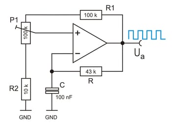
If necessary, a potentiometer (P1) can be inserted between the voltage divider resistors (R1 and R2).
By changing the settings on the potentiometer, the frequency of the astable multivibrator can be changed within a certain range.
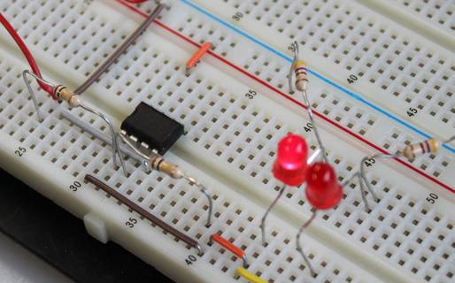
Like the NE555 timer, the LM358 integrated circuit from the operational amplifier category is ideal for educational applications. In combination with a breadboard, the most amazing circuits can be created quickly and easily. According to the data sheet, the manufacturer allows for a wide range of power supplies, so that power can be supplied via battery or power supply unit without any problems.
Despite extensive tasks, very few additional components are often required for the external circuitry. The effects can be measured very nicely when components such as resistors or capacitors are changed.
This allows the circuits on the breadboard to be perfectly optimized and then later replicated for use on perforated circuit boards.
By the way: Depending on the manufacturer, the IC data sheet may list other interesting example circuits that are just begging to be replicated.
