NE555 circuits » Structure and function of the timer explained
Updated: June 15, 2022 | Reading time: 7 minutes
This text is machine translated.
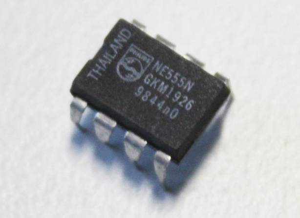
There is probably no other integrated circuit that has been on the market for as long and sold as often worldwide as the NE555 timer. The timer, or NE555 timer IC (integrated circuit), was developed by Swiss engineer Hans R. Camenzind at the US company Signetics and was launched in 1972. We will show you how the NE555 timer works and explain why it is so popular with engineers, circuit developers, and hobbyist electronics enthusiasts.
In principle, the NE555 integrated circuit is an electronic component whose output can be switched on and off under certain conditions. This makes the component ideal for time control or as a clock generator.
Just a few months after its market launch, sales figures exceeded expectations. As a result, the 555, as some technicians often referred to it, was also replicated by other companies. Depending on the manufacturer, the copies were given names such as MC1455, LM555, KA555, or SN72555.
Depending on the external circuitry, the timer can perform a wide variety of complex tasks. Its areas of application therefore range from simple children's toys to high-end applications in space travel.
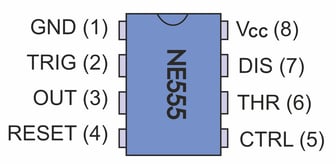
Pin assignment of the NE555
| 1 (GND) = Ground or negative potential of the supply voltage (Vcc). |
| 2 (TRIG) = Trigger input: The output signal rises to the operating voltage (Vcc) when the value falls below 1/3 of the operating voltage. |
| 3 (OUT) = The output is switched by the IC either to the operating voltage (Vcc) or to ground (GND). |
| 4 (RESET) = When the connection is switched to ground (GND), the NE555 interrupts the time interval. |
| 5 (CTL) = Control: Influence on the internal voltage divider. |
| 6 (THR) = Threshold: If the value is greater than 2/3 Vcc, the time interval is terminated. |
| 7 (DIS) = Discharge: Open collector output for switching tasks. |
| 8 (Vcc) = Supply voltage (usually 4.5 - 15 V). In the CMOS version, the timer operates at voltages as low as 1.2 V. |
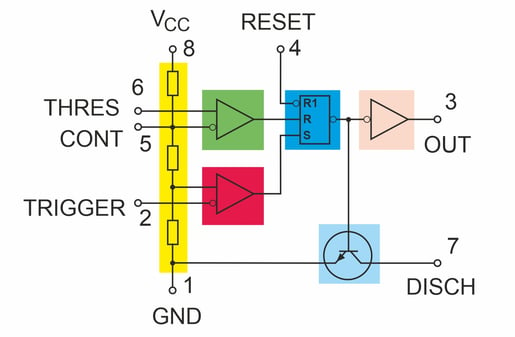
The internal structure corresponds to an arrangement of 24 transistors, 2 diodes, and 15 resistors. These components form 6 functional blocks, which are represented in different colors:
Voltage divider (yellow):
The voltage divider consists of three identical resistors. As a result, the voltage between the resistors can be tapped at 1/3 Vcc and 2/3 Vcc.
Comparators (red and green):
A comparator or operational amplifier compares two input voltages. The output signal then indicates which of the two voltages is higher. One input of each of the two comparators is connected to the voltage divider. The other two inputs correspond to the THR and TRIG connections. These are used to control the timer IC via external circuitry.
Flip-Flop (blue):
A flip-flop is a bistable switching stage that can assume two stable states of the output signal depending on the two input signals.
The states are maintained as long as the operating voltage is applied. In addition, a RESET input ensures that the flip-flop can be reset independently of the input signals.
Output stage (pink):
The output stage amplifies the signal from the flip-flop, enabling currents of up to 200 mA. The voltage potential at the output is either Vcc or GND (ground).
Transistor stage (light blue):
An internal switching transistor is arranged parallel to the output stage. This transistor switches the DIS connection to ground (GND) when the output has a LOW level.
Depending on the external circuitry, the NE555 timer module can be used for various electronic circuits and functions:
Monostable flip-flop:
A monostable flip-flop (monoflop) has only one stable state. An external control pulse is required to change the state.
After a certain time, which depends on the external circuitry, the monostable flip-flop automatically returns to its initial state. This generates a single pulse at the output. This function is required for timers, frequency dividers, capacity measurement, and pulse width modulation.
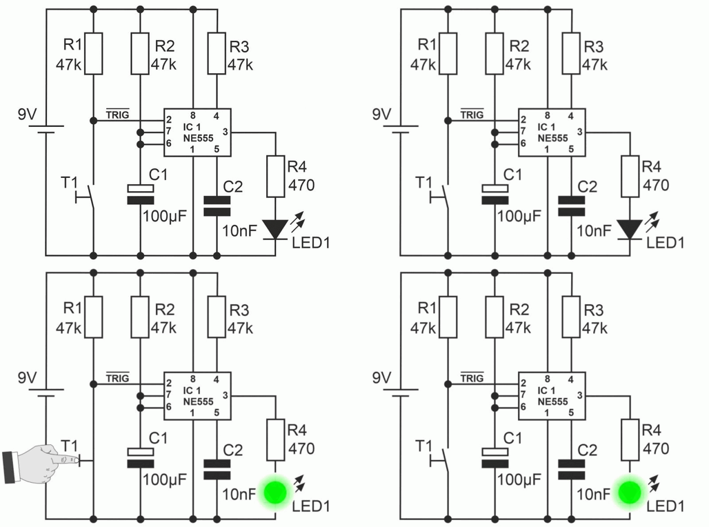
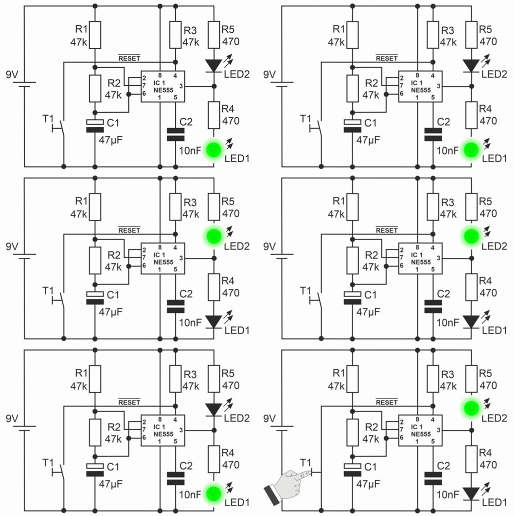
After switching on, the voltage at the trigger input (2) is higher than 1/3 Vcc. This causes the output of the NE555 (3) to be switched to GND potential. The LED1 at the output (3) does not light up. At the same time, the internal transistor stage in the NE555 switches the PIN “DIS” (7) to ground (GND). The external capacitor C1 is thus short-circuited and cannot be charged. The circuit is in a stable state at this moment.
When button T1 is pressed, the voltage at the trigger input (2) drops to 0 V and thus below 1/3 Vcc. The voltage at the output (3) rises to the operating voltage (Vcc level). LED1 lights up. This blocks the switching transistor inside the NE555 and capacitor C1 can now be charged via resistor R2. This switching state is maintained even when button T1 is released and the voltage at the trigger input rises again.
Only when the capacitor has charged to such an extent that the voltage at the THR input (6) is greater than 2/3 Vcc is the output (3) switched back to ground. LED1 goes out. Now the transistor stage in the NE555 is also conductive again, causing capacitor C1 to discharge.
The circuit has returned to its stable state and is waiting for the next negative control pulse at the trigger input (2). Since the pulse must be negative, the input trigger is marked with a strikethrough in the circuit diagram.
Note:
The pulse length at the output can be individually adjusted by changing components R2 and C1. Capacitor C2 serves only as a filter capacitor for the internal reference voltage in this circuit. If high switching accuracy is not required, the capacitor can be omitted without replacement.
Bistable flip-flop:
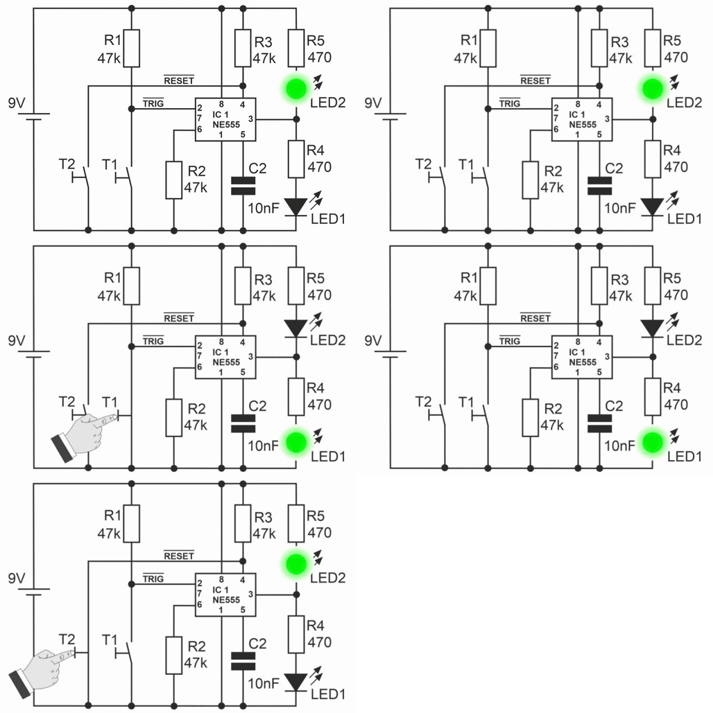
A bistable flip-flop has two stable states that are switched using control pulses. Only the flip-flop built into the NE555 is used for this function.
When the operating voltage Vcc is switched on, the voltage at the trigger input (2) is higher than 1/3 Vcc. This switches the output of the NE555 to GND potential and LED2 lights up. Resistor R2 ensures that the voltage at the THR input (6) cannot rise above 2/3 Vcc. The NE555 cannot therefore switch over and remains permanently in this switching state.
As with the monostable flip-flop, the trigger input (2) is also used for control in the bistable flip-flop. When button T1 is pressed, the voltage at trigger input (2) drops to 0 V and thus below 1/3 Vcc. The voltage level at the output changes to the operating voltage (Vcc). LED2 goes out and LED1 lights up.
The switching state is retained even when button T1 is released and the voltage at the trigger input rises again.
To reset the flip-flop, a brief voltage drop at the RESET input (4) is required. This is achieved by pressing button T2. The output (3) is then switched to ground potential. LED 1 goes out and LED 2 lights up again. This state is maintained until button T1 is pressed again at the trigger input (2).
Astable multivibrator
When the NE555 timer module is operated as an astable multivibrator, it automatically switches between two switching states. It thus functions as an oscillator and generates a square wave voltage at the output.
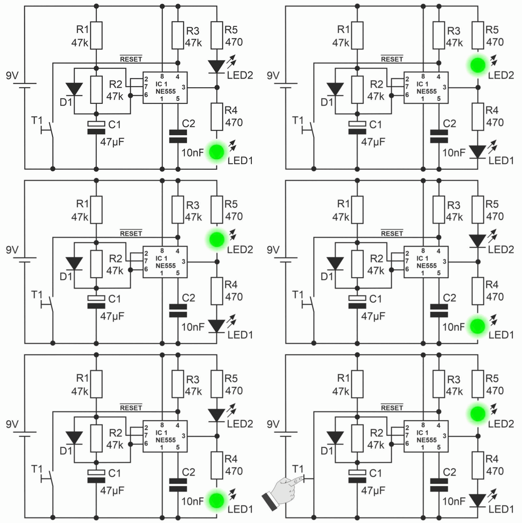
When the power is switched on, capacitor C1 is still uncharged. As a result, the voltage at the trigger input (2) is less than 1/3 Vcc. This means that the operating voltage Vcc is present at the output (3). LED1 lights up. The internal switching transistor blocks and capacitor C1 is charged via resistors R1 and R2. When the voltage at the capacitor, and thus also at the THR input (6), has reached 2/3 of the operating voltage Vcc, the output (3) is switched to ground potential. LED1 goes out and LED2 now lights up.
At the same time, the internal switching transistor also becomes conductive. The DIS input (7) now has ground potential and capacitor C1 is discharged via resistor R2. When the voltage at the capacitor falls below 1/3 of the operating voltage Vcc, the NE555 switches back automatically and a new cycle begins.
If necessary, the timer can be stopped using button T1. When the button is released, the LEDs start flashing alternately again.
The switching frequency and the ratio between the on and off pulses can be adjusted. This can be freely defined using components R1, R2, and C1.
Note:
Capacitor C1 is charged via resistors R1 and R2, but discharged only via resistor R2.
This means that this circuit cannot generate an output signal in which the switch-on time and switch-off time are identical.
However, if both resistors are of equal size and a diode D1 is connected across R2, equal switching times are achieved. This is because the capacitor C is now charged via the resistor R1 and the diode D1. The diode has a low resistance in the forward direction, which can be neglected at this point.
During discharge, the diode blocks the discharge current so that it only flows via the resistor R2.
| Operating voltage: | 4.5 – 16 Vcc |
| Operating current: | 3 – 6 mA (at 5 Vcc) |
| 10 – 15 mA (at 15 Vcc) | |
| Max. output current: | 200 mA |
| Max. power dissipation: | 600 mW |
| Min. power consumption: | 30 mW (at 5 Vcc) |
| 225 mW (at 15 Vcc) | |
| Operating temperature: | 0 – 70 °C |
