74HC595 Shift register » Structure and function clearly explained
Updated: 22.06.2022 | Reading time: 8 minutes
This text is machine translated.
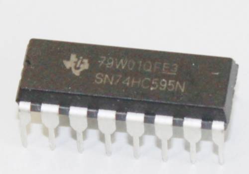
The 8-bit shift register 74HC595 belongs to the large group of integrated circuits (ICs) and is very popular with electronics engineers. This is because a shift register can convert serial data into parallel data as a port expander. This means, for example, that the number of connecting lines between control electronics and a diode display can be kept as low as possible. We will show you how the 74HC595 shift register works in theory as an interface converter and how the control of up to 8 LEDs connected in parallel is carried out correctly in practice.
This question is easiest to explain in connection with a single-board computer. If, for example, you want to control eight low-current LEDs simultaneously with an Arduino or Raspberry Pi, eight outputs are required on the computer board. Although this is technically possible, it is unfortunately not always practical. Especially if the control computer only provides a limited number of outputs.
This is where the shift register comes into play. In the case of the 74HC595, 8 LEDs can easily be connected in parallel and controlled serially by the Arduino or Raspberry Pi. Only three line connections are then required for data transfer from the single-board computer to the shift register. One line is used for the serial transmission of information about which LEDs are to light up and the other two lines are used to control the shift register.
The shift register is an integrated circuit, also known as an IC (Integrated Circuit). To understand the function of the shift register, you first need to take a closer look at the connections (pins).
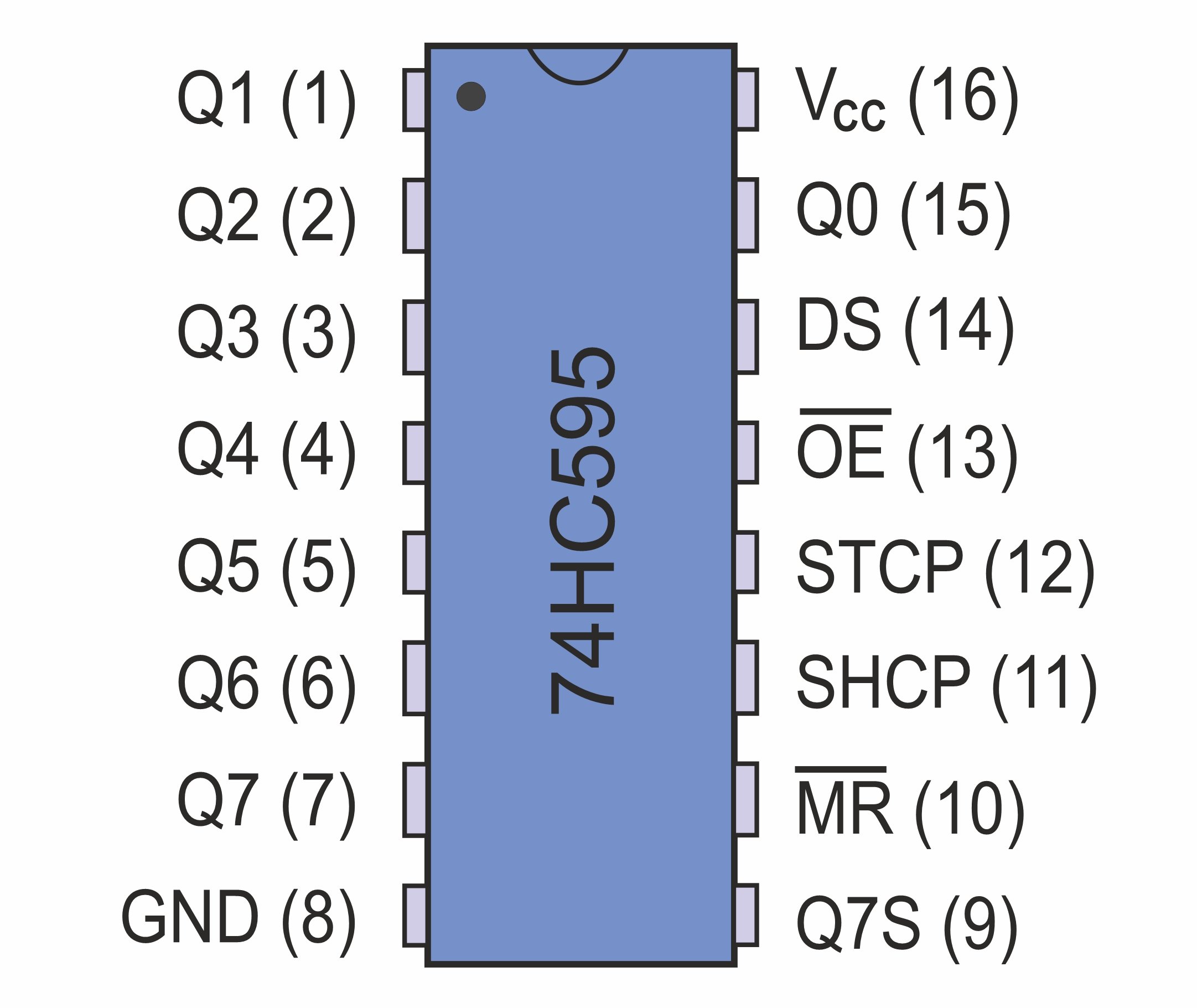
The component has 16 connections (pins) and a semi-circular marking on one of the two narrow sides. The first connection (pin 1) is located to the left of the marking and is marked with a dot. The pins are assigned as follows:
| Q0 to Q7 = Parallel switched outputs |
| Vcc = Plus connection of the supply voltage |
| GND = Minus connection of the supply voltage |
| OE= Output Enable for activating the outputs Q0 -Q7 |
| DS = Data Signal (serial data input) |
| SHCP = SHift Clock Pin is the clock input for transferring the data signal to the actual shift register. |
| STCP = STore Clock Pin - The change from low to high copies the content of the shift register into the output register or output |
| MR= Master Reset for clearing the shift register |
| Q7S = Overflow for possible cascading |
Note:
Depending on the manufacturer, the pins are also labeled with other designations. However, this does not affect the functionality of the IC or the assignment of the connections.
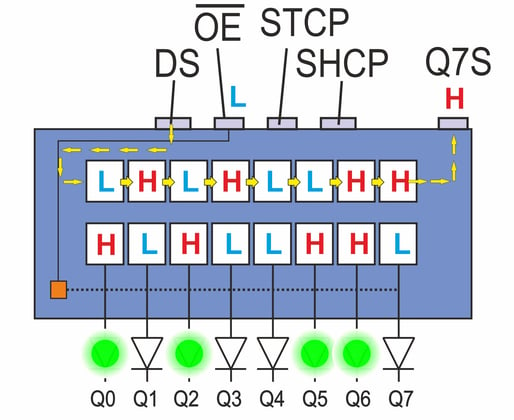
To understand the function of the shift register, imagine a series of eight memory blocks, each of which can store a switching state or a bit (low or high). They are numbered from 0 to 7 from left to right.
Data input
Loading the first bit
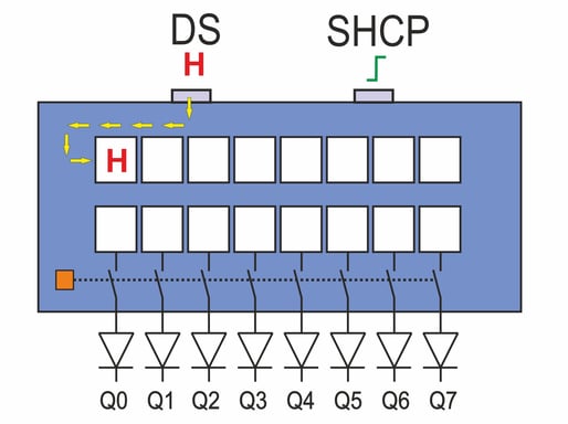
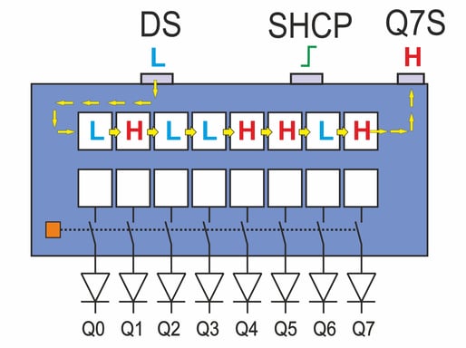
The control or data input into the shift register takes place via the DS connection. The data that is output serially by an Arduino, for example, is available there either as a high (H) and low (L) pulse. The command to save is issued via a positive clock edge on the Shift Clock Pin (SHCP).
As soon as a voltage jump from low to high occurs at this connection, the contents of the 8 memory blocks of the shift register are shifted one position to the right.
At the same time, the current value of the data input (low or high) is written to the first memory block (left). In the example shown, it was a high level.
To be able to save another bit, the voltage on the SHCP pin must first be switched back to low.
Moving the bits
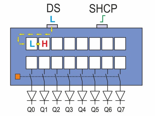
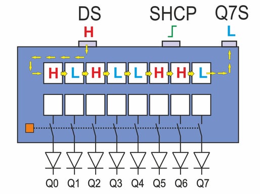
With the next positive voltage jump at the SHCP input, all the contents of the shift register are shifted one position to the right again.
The current level of the DS input is stored in the memory space on the left-hand side that becomes free as a result.
If a low pulse (L) is present at the DS input, this value is now stored in the first memory block.
The voltage at the SHCP must now be switched to LOW again so that further data can be stored.
Complete assignment of the shift register
The processes described above are now repeated until all eight memory locations in the shift register are occupied.
The sequence of the low or high memory states then corresponds exactly to the data sequence at the DS input at the moment of saving.
Important:
The value of the rightmost memory location (memory location 7) is also output at output Q7S.
Data overflow
Cascade function
The next time the voltage at the SHCP input jumps from low to high, the contents of all 8 memory blocks are shifted one position to the right again.
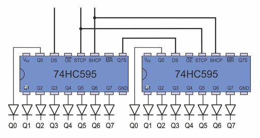
This would result in the information of the rightmost memory location being lost because it is overwritten. However, as the information is output at pin Q7S at the same time, the Q7S connection can be connected to the DS input of another 74HC595 if required (see connection diagram below).
If both ICs receive a common SHCP pulse from the Arduino, the information is not lost but is written as the first bit in the second shift register IC.
Using this method, several shift register ICs can be connected together to form cascades.
Data storage
Data transfer to the output register
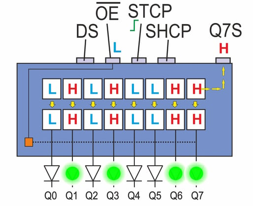
So far, only the shift register has been filled with data. However, the shift register is not directly connected to the outputs of the IC. Otherwise, the outputs would switch uncontrollably with every shift operation.
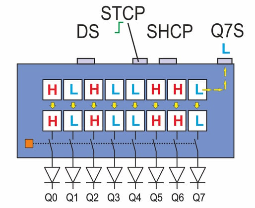
For this reason, the content of the shift register is shifted to the output register or output register (latch).
This is done using the STCP connection. In the event of a positive voltage jump or a positive edge, the data is copied from the shift register to the output register.
The output register works as an 8-fold flip-flop (8-fold latch) and saves the eight switching states of the shift register.
Note: In electronics, a toggle stage that can assume two stable states is also referred to as a flip-flop.
Even if the voltage at the STCP connection later drops back to the ground potential, the data in the output register is retained. Even if the data in the shift register changes, this has no effect on the output register. The data in the output register is not overwritten until the next positive voltage jump at the STCP input.
Enable outputs
Activate IC outputs
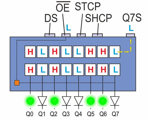
The outputs must be switched on for the signals to be available at the output. This is done via the OE connection.
If this connection is switched to the earth potential (GND) with a resistor, the outputs are activated (low active) and the connected lamps or rather LEDs light up.
If the OE connection is set to high, the outputs are high-impedance.
As a result, the outputs have three possible states (tri-state output): High, Low or high impedance.
The fact that the connection must have a LOW potential for the outputs to be activated is expressed by the overline next to the pin name.
Data shift between shift and output registers
Once the output register has been filled, new data can be shifted into the shift register according to the system shown above.
Even if the data in the shift register changes, the data in the output register and the lighting scheme of the LEDs remain unaffected.
This means, for example, that the previous LED pattern is still displayed in a ticker display, while the new data is already loaded into the shift register.
Delete data
Delete shift register
If required, the data in the shift register can also be deleted.
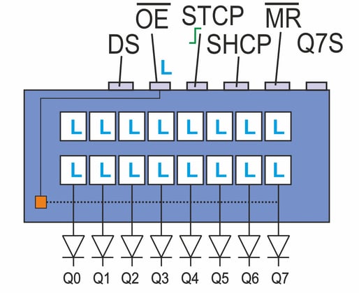
The MR (Master Reset) connection is used for this purpose. This connection is usually connected to the supply voltage via a resistor. This means that the connection is continuously at a high level.
If the connection is switched to the ground potential (GND or low), the data in the shift register is deleted.
As a low potential must be applied to this pin (low active) in order to delete the data, the designation of the reset connection is also provided with an overline.
Delete output register
To also delete the data in the output register, a positive voltage jump must be applied to the STCP connection.
This overwrites the switching states in the output register and the connected LEDs go out.
The shift register is now back in its initial state.
When connecting the shift register, the manufacturer's technical data must always be observed. In particular, the operating voltage (Vcc) of 2 - 6 V and the maximum output current of 35 mA must be observed.
For this reason, low current LEDs must always be used if the LEDs are controlled directly by the shift register. If you want to operate loads with higher power, you must switch transistors with the outputs or use a switching module.
However, other circuits from the field of digital technology can also be connected directly to the outputs of the 74HC595.
Cascade connection
As already mentioned, several ICs of type 74HC595 can be connected in series.
The output Q7S of the upstream IC must be connected to the input DS of the downstream IC.
The number of ICs that can be cascaded is theoretically unlimited.
However, the more ICs are connected in series, the longer it takes until all memory locations are shifted by one position.
In most practical applications, the number of shift registers connected in series is limited, so the time factor does not play a major role in this case.
