ULN2803 » Structure and function of the switching module clearly explained
Updated: June 28, 2022 | Reading time: 6 minutes
This text is machine translated.
When it comes to switching multiple display LEDs or loads of different sizes with a single-board computer, the ULN2803 switching module is a popular choice in electronics. The reason for this is its significantly simpler circuit design. We show you how the driver IC or switching module works and how to connect it correctly.
In digital switching technology, powerful signal lamps or various relays often need to be controlled. Since the outputs of digital circuits are largely unable to switch these consumers directly, so-called switching transistors must be used. In the case of an 8-channel running light, this means 8 switching transistors, 8 light-emitting diodes, and 8 series resistors. If inductive loads such as relays need to be switched, an additional free-wheeling diode is required for each coil.
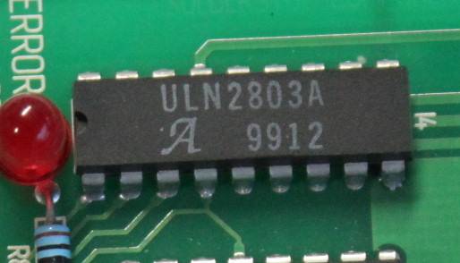
Sure, the components are not necessarily expensive, as most of them cost only a few cents. Rather, the significant space requirement is the big problem. And this is exactly where the ULN2803A switching module shows its strengths. The integrated circuit (IC) contains 8 switching stages, including the associated free-wheeling diodes.
Despite its compact design, each of the 8 switching stages can switch currents of up to 500 mA. However, the switching voltage can also be set quite high if required. This is because the voltage resistance of the outputs is up to 50 volts (V).
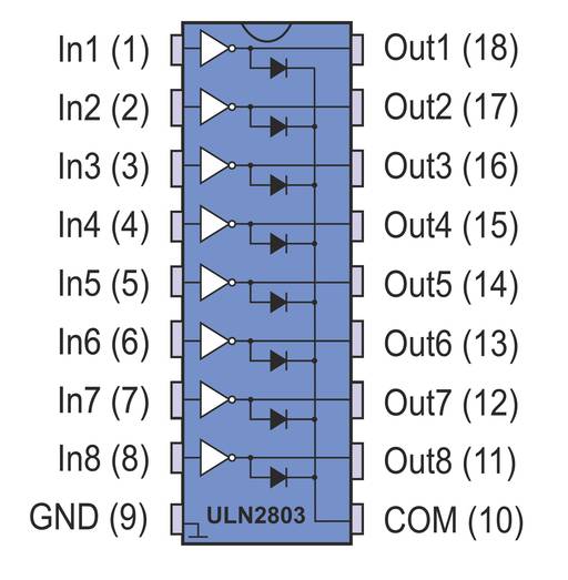
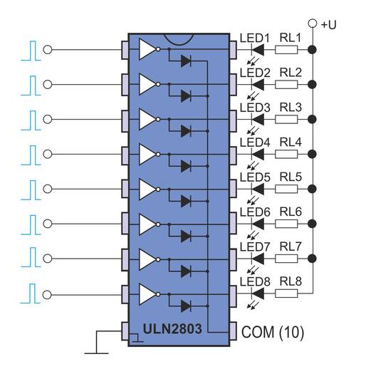
The term “switching module” indicates that this IC must contain several integrated electronic switches. And that is exactly the case. The driver IC contains a total of 8 switching stages, each of which connects an input to the opposite output. This greatly simplifies the circuit board layout.
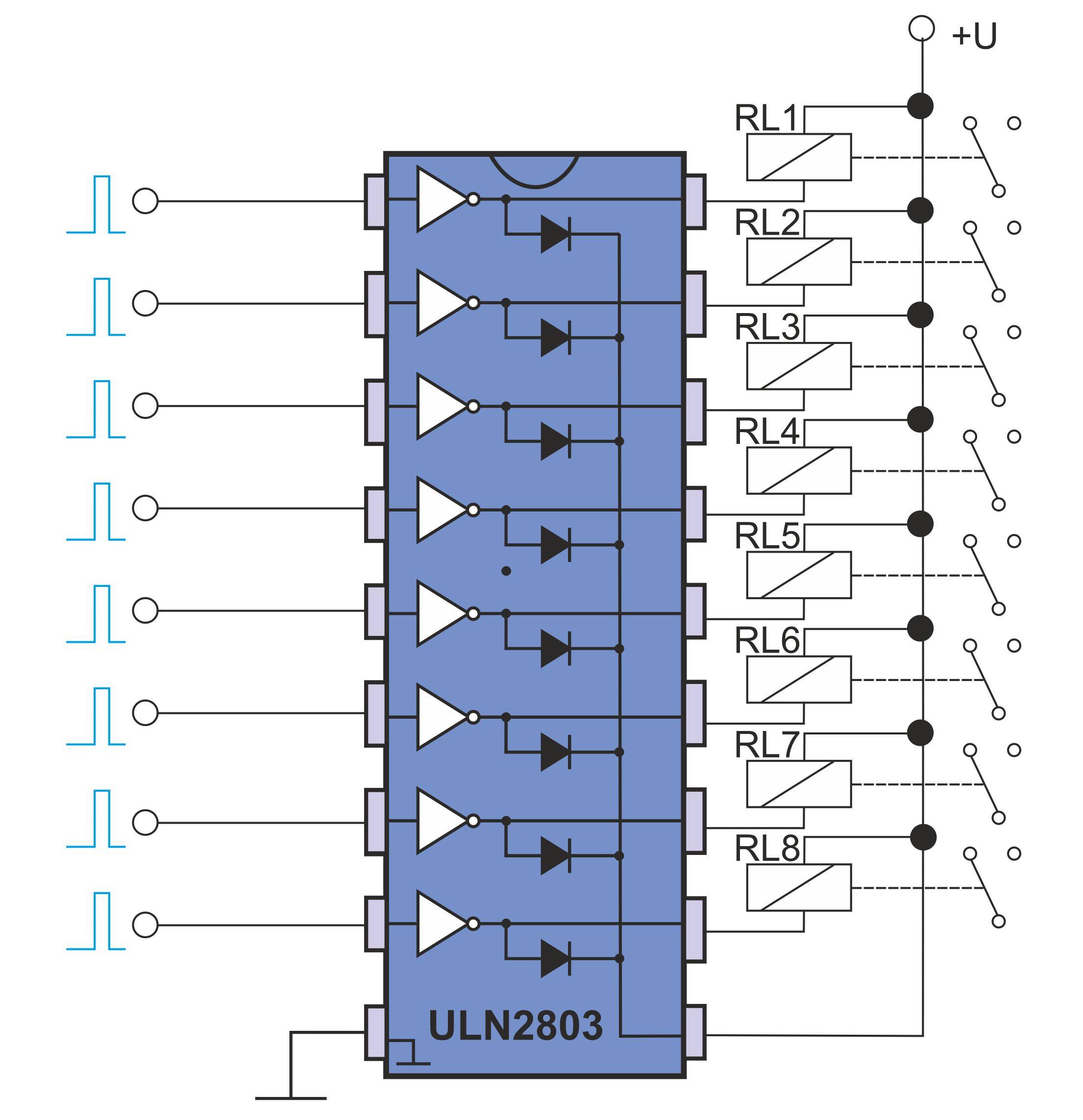
Since even a small control current is sufficient to switch a higher load current, this current amplification is represented as a triangle. We explain what the small circle after the triangle means in the following section on the function of the IC.
Each output of the IC is additionally connected to the common COMMON connection (COM) via a separate free-wheeling diode. The ULN2803A is available with a DIL-18 housing or as an SMD component.
The ULN2803 has a semicircular marking on one of the two narrow sides of the housing. When the component is oriented with the marking facing up, pin 1 is located to the left of it.
Pin 1 is also the input of the first switching stage. The pins are numbered counterclockwise. Consequently, the output of the first switching stage is located on pin 18.
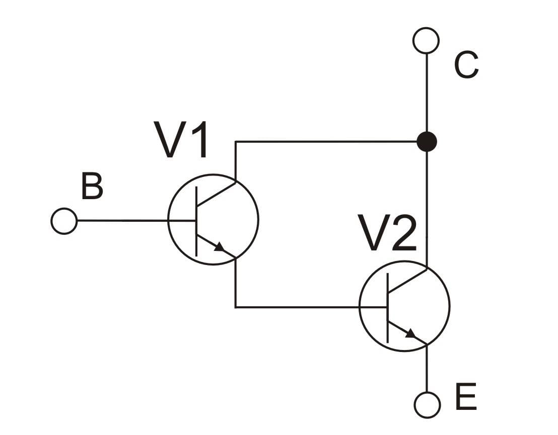
Two transistors arranged in a Darlington circuit serve as current amplifiers or electronic switches. For this reason, the component is sometimes referred to as the ULN2803A Darlington transistor array, switching transistor array, or simply as a transistor array.
The term transistor array simply refers to the arrangement of transistors in a row. In addition to transistor arrays, there are also resistor arrays, which contain several resistors. And in rectifier diode arrays, several diodes are housed in a single package.
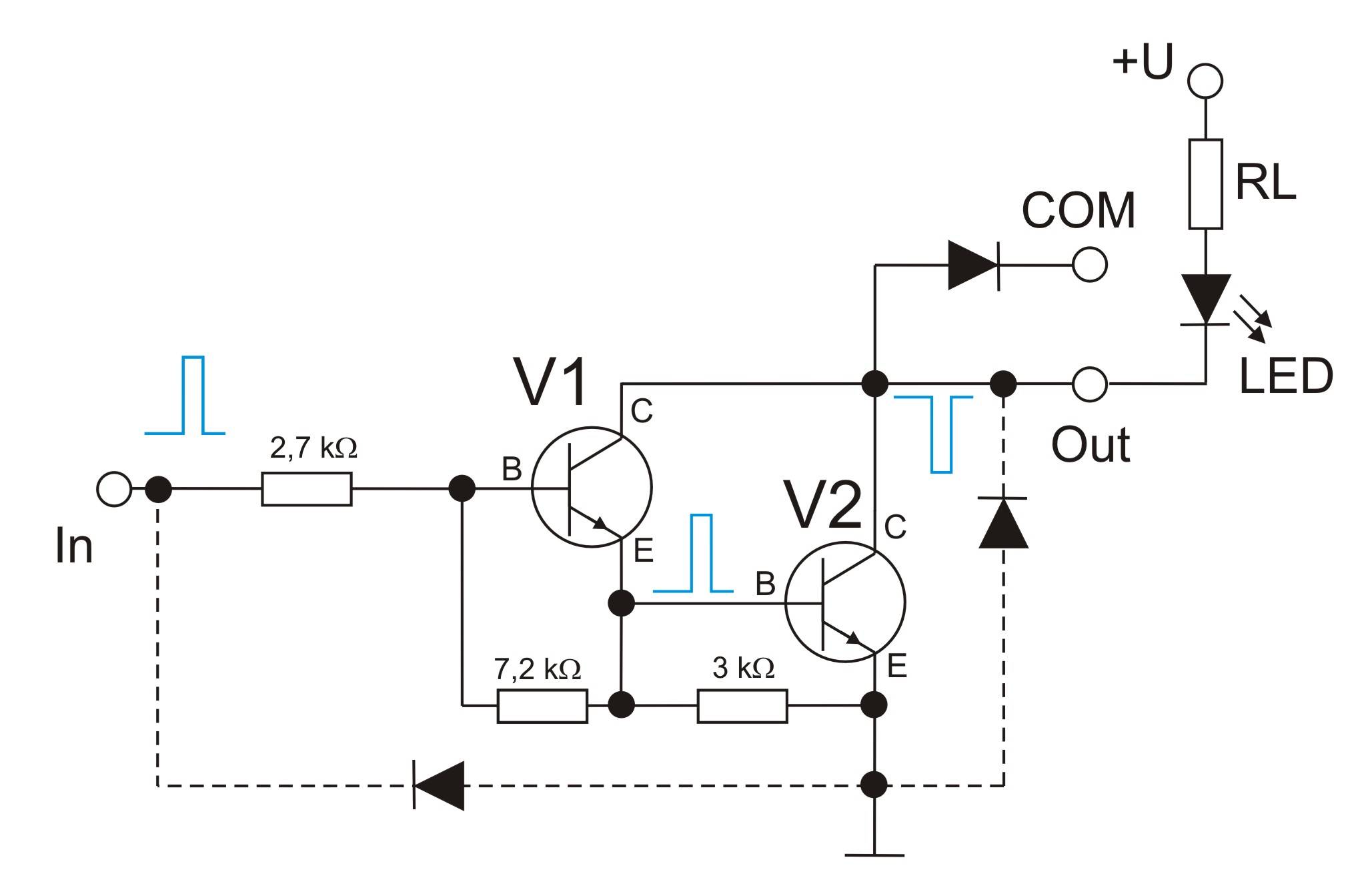
A Darlington circuit consists of two bipolar transistors. The left transistor (V1) functions as an emitter follower, resulting in a very high input resistance.
The right transistor (V2) functions as a power transistor, which is responsible for the high switching currents.
This allows a high load current to be switched with a low control current.
In a Darlington transistor, the two transistors are housed in a single package. However, in a Darlington transistor with silicon technology, the base-emitter voltage doubles to approximately 1.4 V. In a standard transistor, it is around 0.7 V.
In a fully switched Darlington transistor, the collector-emitter voltage can still be up to 2 V.
Different designs
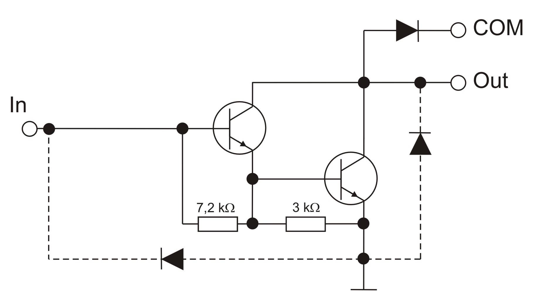
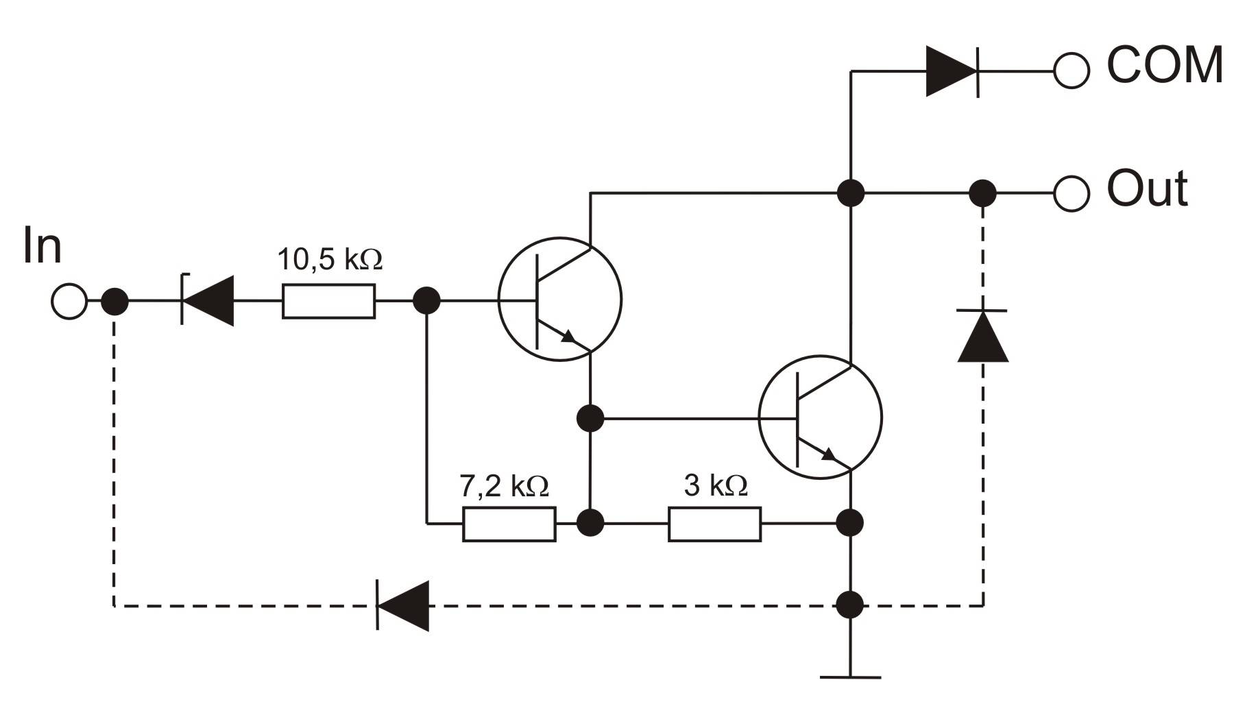
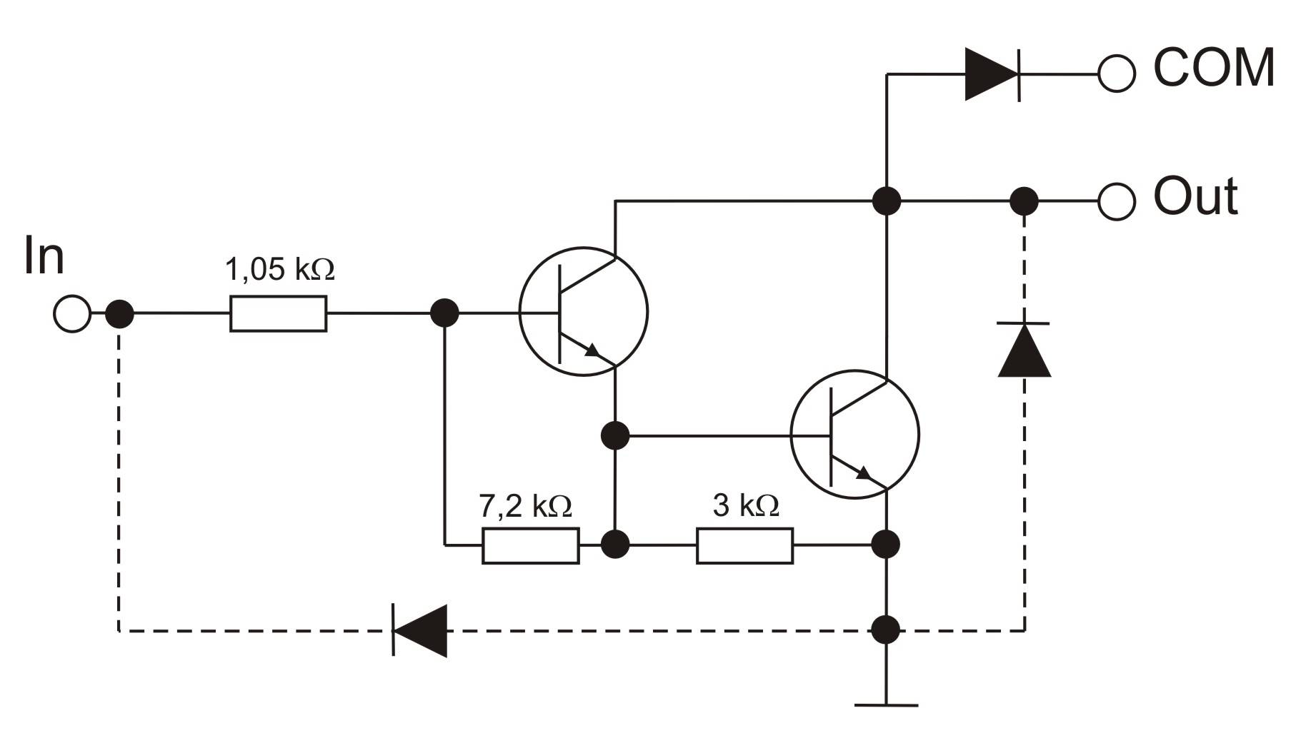
The ULN2803A integrated circuit is a component from a whole series of UNL28XX ICs, which are constructed in the same way and also function in the same way. The small but subtle differences lie solely in the input impedance and usability with other components. As a result, the internal structure of the Darlington circuit is slightly different:
Note:
The diodes with the dotted lines are recommended protection diodes.
The function of a Darlington switching stage in the ULN2803 switching module can be explained quite simply using the principle circuit diagram:
Without a control signal at the input, the two NPN transistors V1 and V2 are blocked and the LED at the output does not light up. Since no current flows, no voltage drops across the series resistor and the LED, and the full operating voltage +U is present at the output (Out).
If a positive pulse is now applied to the input (In), it is forwarded to the base of transistor V1. This causes the collector/emitter path of transistor V1 to become low-impedance. The resulting increase in collector/emitter current causes the voltage at the emitter of V1 to rise. Since the base of transistor V2 is connected to the emitter of V1, the voltage at the base of transistor V2 also rises.
At a value of 0.6–0.7 V, transistor V2 also switches the collector/emitter path to low resistance. The LED begins to light up and the series resistor RL limits the current through the LED.
Note:
Since a positive voltage pulse at the input results in a voltage drop at the output, experts refer to this as the input signal being reversed (inverted). In the schematic diagram of the internal circuitry (see second figure from the top), this is indicated by a small circle after the current amplifier triangle.
Instead of an ohmic load, such as an LED with a series resistor or an incandescent lamp, the ULN2803 switching module can also switch inductive loads such as relays, solenoid valves, or stepper motors. However, the current, voltage, and power must always remain within the permissible limits specified in the data sheet.
The maximum switching voltage is 50 V, and the maximum continuous current per switching stage is 500 mA. The maximum power dissipation per switching stage is 1 W, and the maximum power dissipation of the entire IC is 2.25 W.
If necessary, switching stages can also be connected in parallel, e.g. to distribute the switching currents. Further information can be found in the technical data or the manufacturer's data sheet.
For those new to electronics, it may come as a surprise that the component does not require a supply voltage in the conventional sense. Although pin 9 provides a connection for ground (GND), there is no Vcc pin for a positive connection on the IC.
This is also not necessary, as the NPN Darlington switching transistors receive their switching voltage via the respective consumers. This voltage is then simply switched to ground by the driver.
Connection of inductive loads
If inductive loads such as relays or motors are switched, the COMMON connection (pin 10) must be connected to the positive connection of the supply voltage for the motors or relays. When the switch is turned off, the respective diodes in the IC short-circuit the resulting self-induction voltage.
Important:
If the switching current of an output with a maximum of 500 mA is not sufficient, several outputs can also be operated in parallel to switch a load with a current consumption of more than 500 mA.
Also possible: If necessary, the loads to be switched can be operated at a higher voltage than in the control circuit. If the control electronics are operated at 5 V, relays with a coil voltage of 12 V, for example, can be switched without any problems. In this case, only the ground potential of both circuits must be connected to each other.
Our practical tip
Even though a free-wheeling diode is integrated into the switching module for each channel, development engineers still like to use free-wheeling diodes in the immediate vicinity of the relays or motor connections. This tried-and-tested measure is particularly useful for large inductances.
To test the switching module or the ULN2803 driver IC, you need a signal source that supplies a 5 V control signal. This can be a single-board computer (Raspberry or Arduino), a TTL circuit, or other control electronics.
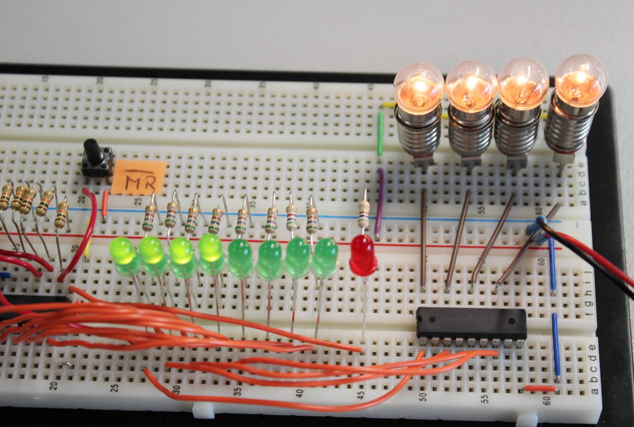
Since the shift register cannot switch high currents, we had to use low-current LEDs for the display. With the help of the ULN2803 driver module, we can now also control bright light bulbs with the shift register.
To keep the layout on the breadboard clear, only four bulbs were used. In addition, the bulbs are connected to the same power supply as the shift register.
The first four outputs of the 74HC595 shift register are connected to the randomly selected inputs 1, 3, 5, and 7 of the switching module.
One bulb is connected to each of the outputs 1, 3, 5, and 7 of the switching module. The second contact of the four bulb sockets is connected to the positive terminal of the supply voltage.
