MEMS » Micro-electro-mechanical systems explained simply
Published: 22.08.2022 | Reading time: 7 minutes
This text is machine translated.
Very few people are familiar with the abbreviation "MEMS" or the term MEMS sensor. However, everyone has certainly experienced the application and practical benefits of a MEMS sensor for themselves. For example, when a simple rotation of a smartphone is enough to make the image shown on the display larger and therefore more visible.
In order to implement this user-friendly solution, special MEMS sensors are required in the phone that can detect rotational movements and accelerations. What is more of a nice gimmick in a smartphone has now become an absolute necessity in many other areas of technology.
This is a good reason for us to take a closer look at MEMS sensors and the technology behind them.
The term "MEMS" is the abbreviation for Micro-Electro-Mechanical-Systems. As the name suggests, a MEMS is a combination of mechanics and electronics in a very small space. The reason for the development of MEMS technology was ultimately a logical consequence of the fact that classic precision mechanics and precision engineering for electronic devices had already reached their limits in the 1980s.
Although conventional machining of materials ideally allowed tolerances of a fraction of a millimeter, this was far too coarse. Especially when complete components and structures are to be produced whose overall dimensions are significantly less than one millimeter. This can only be achieved by combining microelectronics and micromechanics.
In microsystems technology, actuators such as pumps, motors, microphones, loudspeakers and sensors can be manufactured in tiny designs. This technology is even increasingly being used in medicine for biometric sensors.
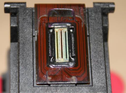
Thanks to MEMS microphones and MEMS loudspeakers, modern hearing aids are extremely discreet and almost invisible. Incidentally, the bubble jet print head of an inkjet printer is also a MEMS-based system.
As the dimensions of the mechanical components of a MEMS are not in the millimeter range (mm) but in the micrometer range (µm), completely new approaches must be taken in production. However, a well-known and already proven technology is used for this purpose. As in the production of semiconductor chips for integrated circuits (ICs), the structures of the MEMS components are built on a slice of silicon (silicon wafer). Various surface micromachining processes are used for the construction and production of MEMS components:
Photolithography
In photolithography, the required areas of the functional layer (1) are protected by a photoresist (2) during the etching process.
This is first applied as a homogeneous layer over the entire surface using the centrifugal process (see top image of the sketch).
During the subsequent exposure of the photoresist (see middle figure in the sketch), a mask (3) is used to sharply delineate required and non-required areas.
If a positive varnish was used, the exposed areas of the photoresist are removed during development (see bottom illustration of the sketch).
With a negative resist, the shadowed areas are removed. The wafer can then be etched.
Etching process
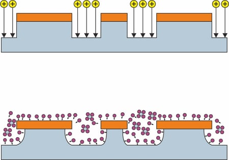
In order to create the required structures in silicon, conventional wet-chemical as well as dry-chemical etching processes are used. Reactive ion etching is a chemical-physical dry etching process that offers special possibilities in the production of MEMS. Positively charged ions are generated in a gas plasma and accelerated in a targeted manner to the negative electrode with the wafers.
On impact, the ions dissolve material from the surface (physical etching). Depending on the direction of movement of the ions, an anisotropic etching profile is created (see figure above).
By changing the process parameters (pressure, plate distance, gas flow or generator power), the behavior of the ions during the etching process can be influenced. They then no longer behave in a targeted manner, but constantly change direction due to collisions.
The etching process is now non-directional (isotropic) and has a chemical character due to the reaction of the free radicals on the surface. As a result, areas protected by the photoresist can also be infiltrated (see figure below).
Separation
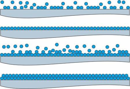
In atomic layer deposition (ALD), uniform atomic layers in the nano range are built up by surface reaction with the substrate. Even complex structures with indentations can be optimally coated with the appropriate procedure. A wide variety of substances are used depending on the required function.
The choice of material depends on whether the electrical, thermal, piezoelectric, magnetic or mechanical properties of the layers are to be utilized.
The deposition can either be selective or the structured functional layer can be produced in a subsequent etching process.
Creation of 3D structures
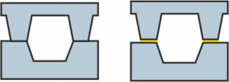
In micromechanical systems, many applications require structures and components that can move to a certain extent. This only works if the structures are appropriately shaped and correctly supported or anchored within the system. SOI wafers (Silicon On Insulator) are used to create three-dimensional movable structures.
Combination of manufacturing processes
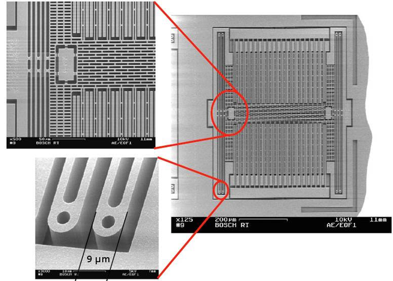
The combination of the above-mentioned manufacturing methods and the multiple deposition and etching of thin structural layers and sacrificial layers make it possible to create a wide range of micromechanical structures and indentations. The dimensions of the individual components achieved are significantly smaller than the diameter of a human hair, which is around 50 - 80 µm.
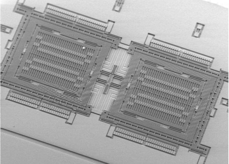
The attached image shows a small section of a MEMS sensor to illustrate the extremely small yet cleanly produced structures.
The mechanical process used in MEMS production ensures rapid manufacture and consistently high quality. In addition, the enormous quantities and low material usage enable cost-effective mass production.
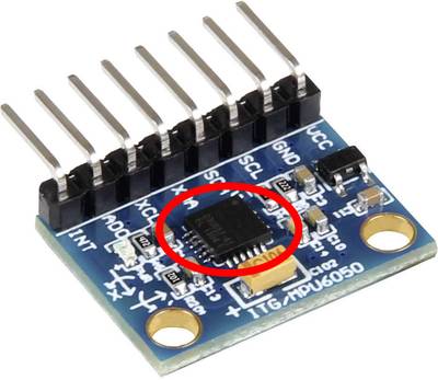
MEMS technology is ideally suited for a wide variety of sensors. MEMS acceleration sensors and angular rate sensors in particular can be realized excellently with MEMS technology. Older sensors could only detect movement in one direction. Modern sensors, such as the MPU-6050 sensor chip, integrate a 3-axis acceleration sensor and a 3-axis rotation rate sensor (gyroscope) in a housing measuring just 4 x 4 mm.
Thanks to its small footprint, this MEMS sensor can be easily implemented in a wide variety of devices. However, this sensor chip is also often used in development or training, as this sensor board for development kits such as Arduino or Raspberry Pi shows.
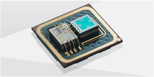
In contrast to this, however, it is also quite common for intelligent sensors that the MEMS mechanics and the evaluation electronics, including the digital signal processing, are independent assemblies.
The individual assemblies are only wired together inside the chip housing when the sensor is manufactured.
Other popular sensors for which MEMS technology is increasingly being used are flow sensors, pressure sensors, temperature sensors and sensors for gases or air quality.
The technology and function of a MEMS sensor can be most easily demonstrated using an accelerometer. In an accelerometer, comb-like micro-structures are created using the production process mentioned above.
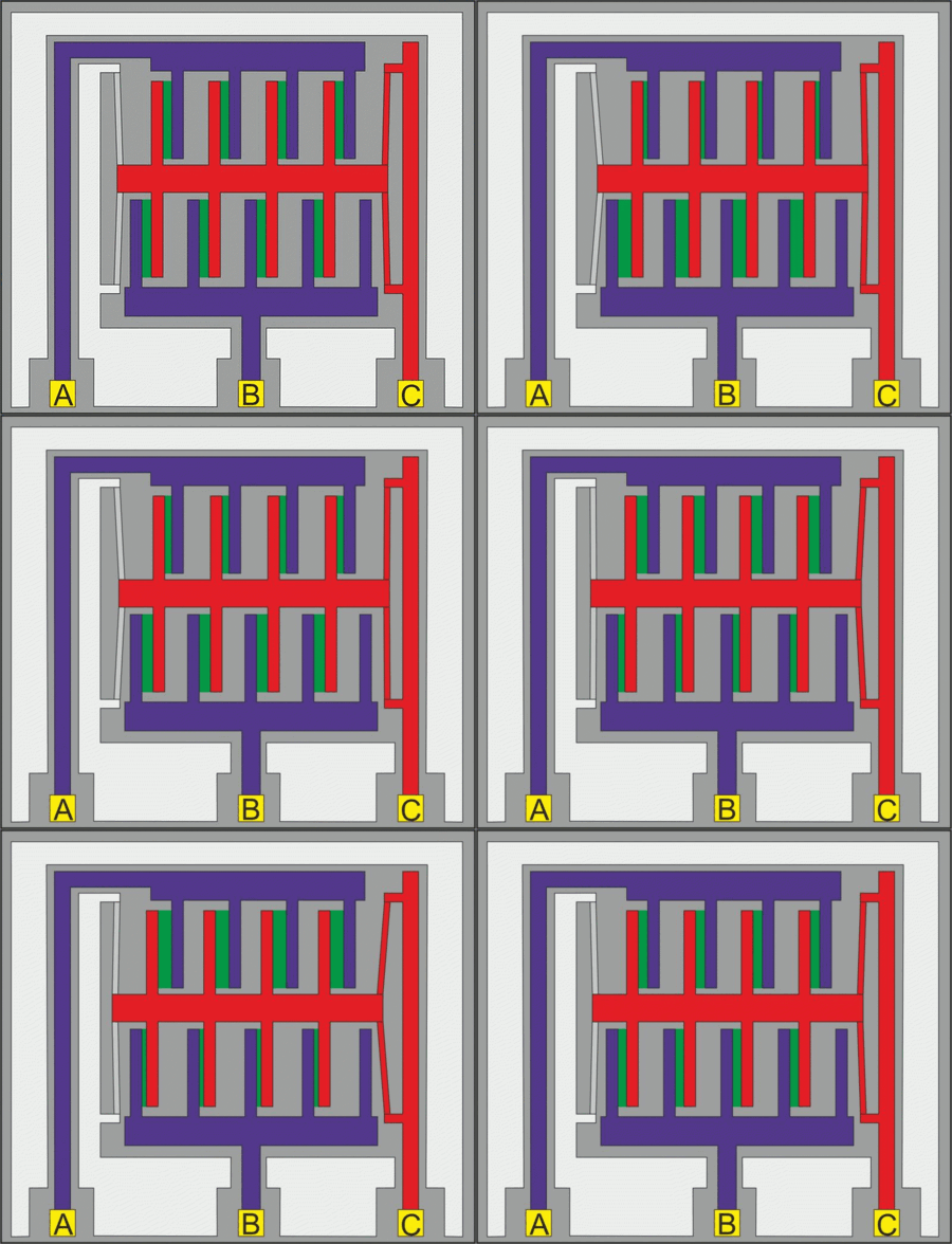
The middle element (1) is a movably mounted mass and is held in the middle position by spring elements (2). The upper comb element (3) and the lower element (4) are firmly connected to the sensor housing.
The interlocking teeth of the combs represent capacitors which, due to their size and the instantaneous distance between the connection points A and C or B and C, have a certain measurable capacitance.
The effective areas of the capacitors are shown in green in the sketch.
The functional principle
Depending on the acceleration or deceleration, a force acts on the accelerometer, which deflects the movable comb structure inside laterally to the left or right.
This changes the relative position of the comb teeth to each other. As a result, the distance between the capacitor surfaces and therefore the capacitance value also changes.
If the distance becomes smaller, the capacitance value increases. If the distance increases, the capacitance value decreases. Depending on how the capacitance changes between the connection points A and C or B and C, the digital electronics of the sensor can determine the strength and direction of the acceleration.
As a result, the image on the smartphone mentioned above is displayed correctly after rotation and not upside down.
Actual structure
The sketches in this section are kept very simple in order to clearly explain the structure and mode of operation. For this purpose, we have also shown the deflection of the moving mass very clearly. The two attached pictures show the actual structure of a MEMS sensor.
The angular rate sensor consists of two acceleration sensors mechanically coupled via a double cross. This makes it possible to detect rotational movements around an axis. This complex process was clearly explained by Bosch in this video.
As already mentioned at the beginning, MEMS sensors are used in many mobile devices and smart devices. In notebooks, for example, acceleration sensors detect a fall so that the read/write head of the HDD hard disk can be moved to the parking position in good time before impact. MEMS are also very popular in automotive engineering. There, for example, they control the ESP function, trigger the airbags in the event of an accident or ensure that navigation continues to work even if no GPS satellites are received in a tunnel.
The advantage of industrial production is that high-quality MEMS sensors are available at very low cost. This is why manufacturers of copters and drones like to use them. Clever MEMS technology is even used in entry-level models to achieve outstanding flight stability.
Camera stabilization with MEMS sensors
With high-quality copter models, the micromechanical stabilization of the camera mount is another useful application. As the rocking movements are automatically compensated for in flight, absolutely smooth and shake-free videos are very easy to create.
The correct electrical measurement of different physical quantities and the electronic processing of the information have always been a particular technical challenge. With MEMS technology, however, a technology is now available that not only enables precise, robust and durable actuators and sensors. Thanks to the nanostructures used and industrial mass production, components are becoming ever smaller, more powerful and more cost-effective. It is no coincidence that the MEMS sector has experienced enormous growth in recent years. As sensor technology plays an important role in almost every area of our technological world, MEMS technology will continue to grow. We, the consumers, will only see so much of this as previously unrealizable functions and performance features suddenly become seemingly effortless in our technical devices.

