LM324 » Design and function of the quadruple operational amplifier explained simply
This text is machine translated.
Updated: 03.08.2022 | Reading time: 5 minutes
Operational amplifiers are active components that are frequently used in electronics. This is because they can be used to easily perform many tasks in control engineering, regulation technology, and amplification technology.
Thanks to their almost ingenious properties, very few external components are required for operation, even for complex requirements.
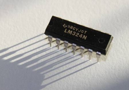
For some tasks or electronic circuits, several operational amplifiers are often required at the same time. For this reason, the LM324 integrated circuit was developed, a component that combines four operational amplifiers in one housing.
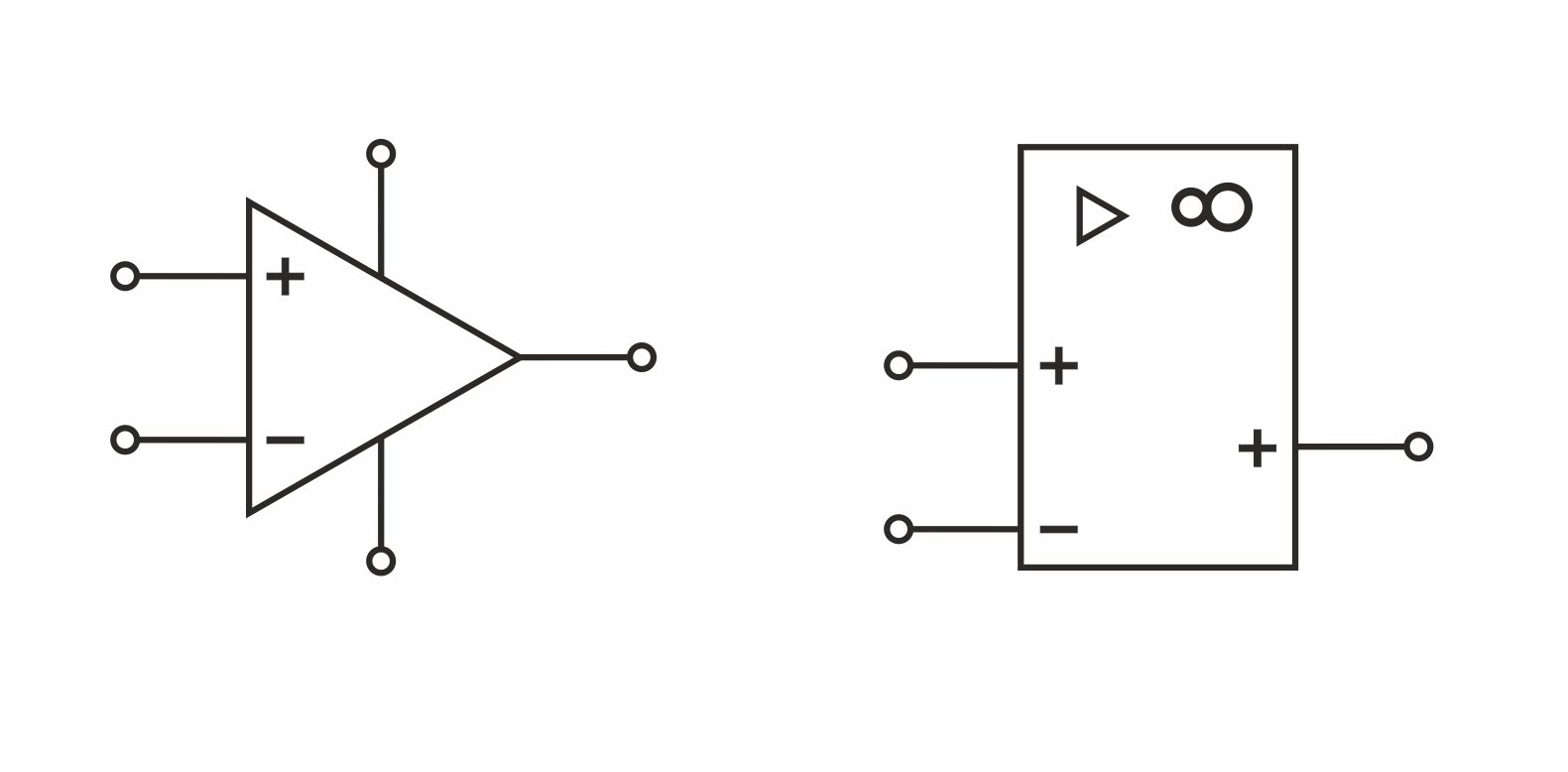
An operational amplifier (OPV) or OP AMP is an electronic circuit that has two different inputs. The special feature of these inputs is that only the voltage differences between the two inputs are amplified.
This is why they are often referred to as differential amplifiers. If both inputs change the voltage level in the same direction at the same time, this has no effect on the output. We have already explained in detail how an operational amplifier works and how to connect it correctly in our article on the OP AMP LM358.
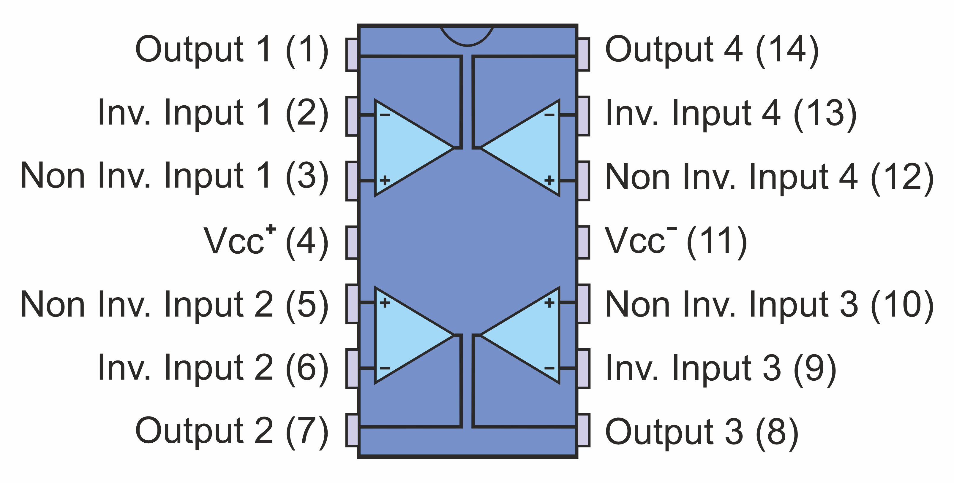
In principle, the OP AMP LM324 is the big brother of the LM358. Unlike the LM358, which has two integrated operational amplifiers, the LM324 has four independently operating OPVs. Another difference is the symmetrical design of the connections.
In addition to the classic IC in a DIP package, the LM324 is also available as an SMD component with different packages or different grid dimensions (SOIC-14 and TSSOP-14). Some manufacturers even offer a square design (QFN16) as an option.
Further information on the different designs, including images, can be found in the manufacturer's data sheet.
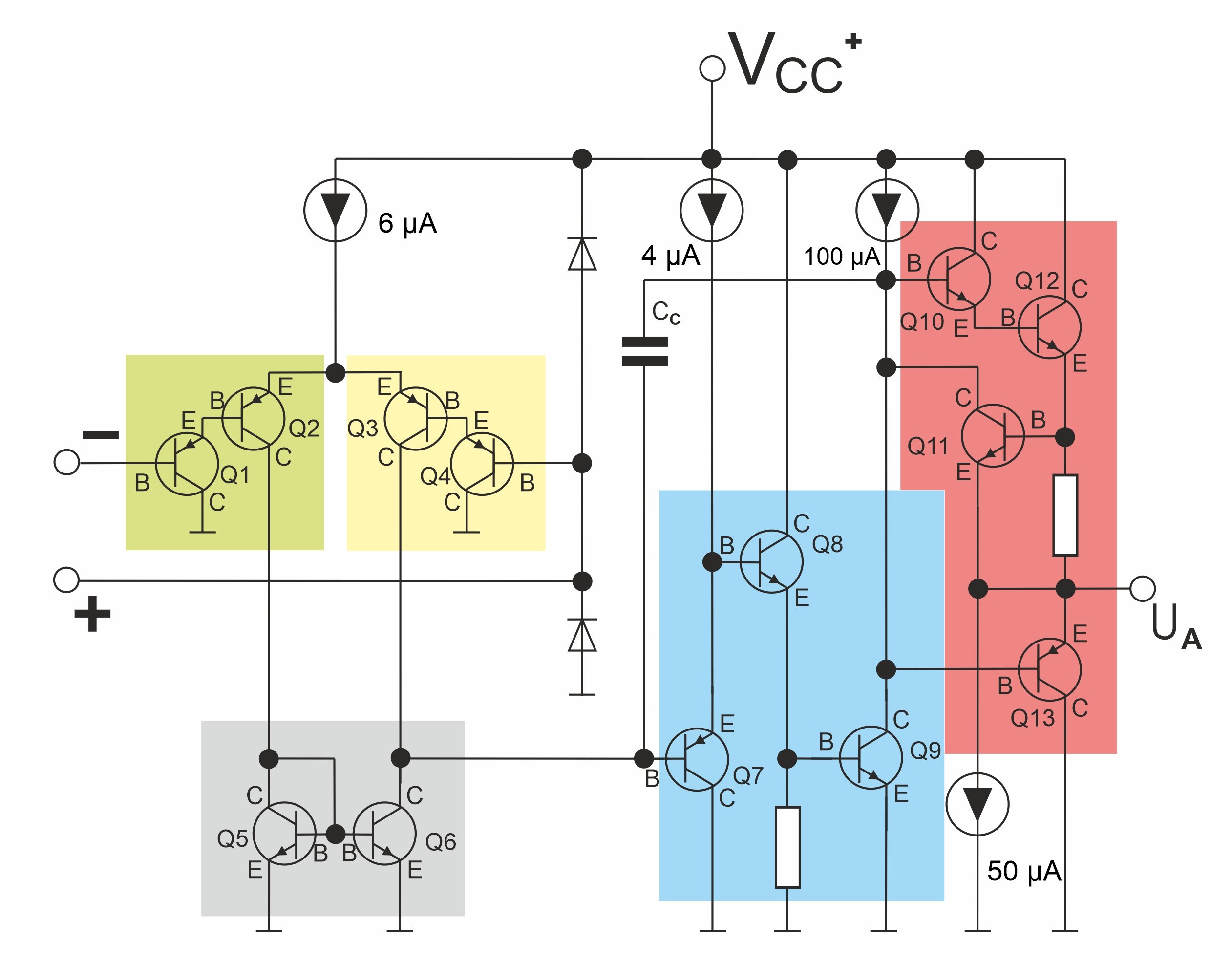
To understand how an op-amp works, you need to familiarize yourself with the basics and take a closer look at the schematic diagram of one of the four operational amplifiers.
Basic structure
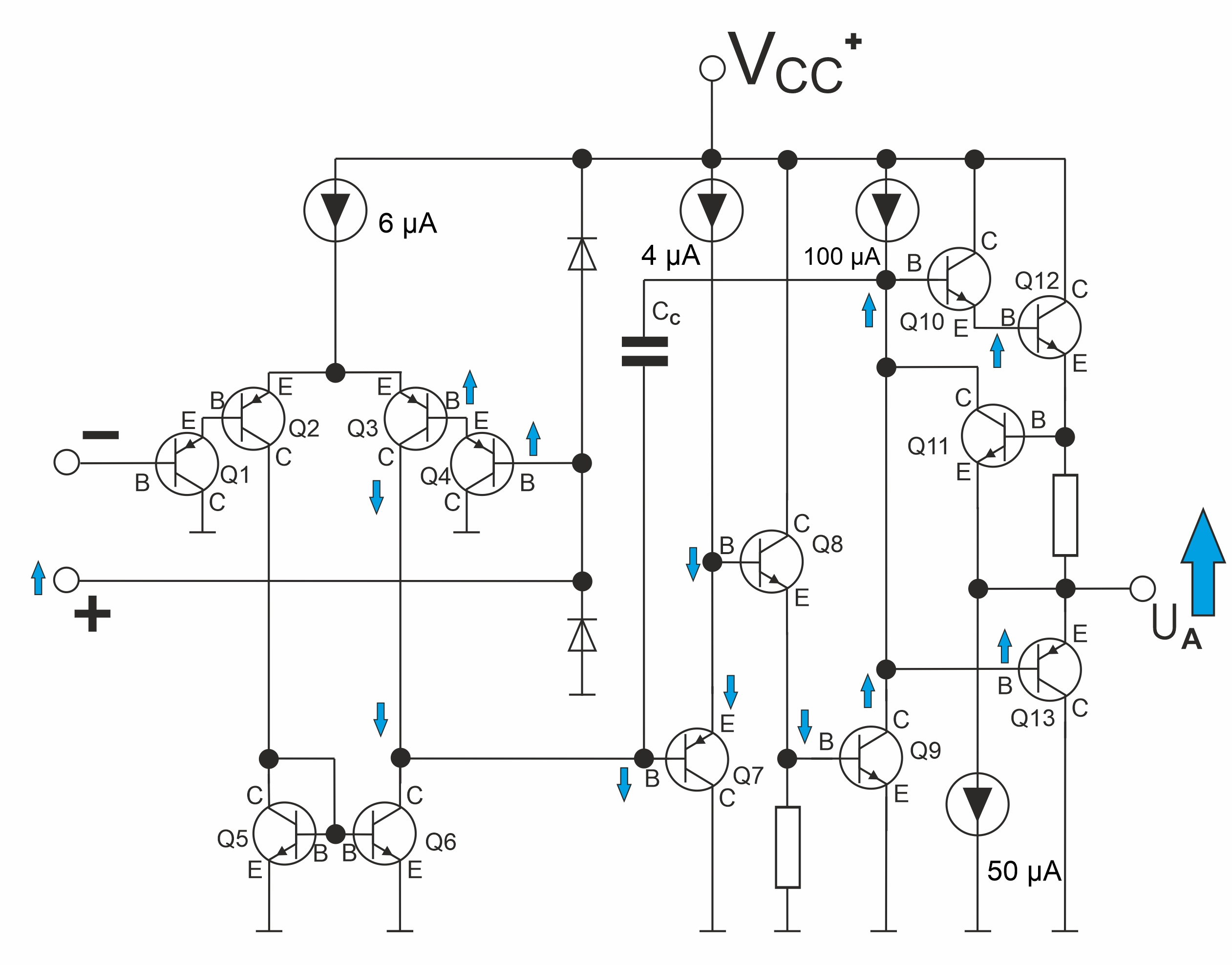
Transistors Q1 and Q2 (light green) are the input transistors for the inverted input (-). Transistors Q4 and Q3 serve as input transistors (yellow) for the non-inverted input (+). Transistors Q5 and Q6 function as current mirrors (gray), whereby the collector/emitter current of Q6 is always equal to the collector/emitter current of Q5.
The control signal for the preamplifier is tapped at the collector of Q6. Transistors Q7 to Q9 serve as preamplifiers (blue) and control the output stage (pink). The output stage consists of transistors Q10 to Q13. Transistor Q12 switches the output to the positive voltage potential of the operating voltage and transistor Q13 switches the output to the negative voltage potential of the operating voltage (GND).
If the current flow via Q12 becomes too high, transistor Q11 switches the control signal to ground (GND). This protects the output stage from overload. Capacitor CC is used for frequency compensation.
The integrated circuit can be operated at a supply voltage of 3 to 32 V. With a dual supply, the supply voltage can be ±1.5 V to ±16 V. Several integrated constant current sources (shown as a triangle in a circle in the schematic diagram) ensure optimum supply to the transistor stages at a wide range of operating voltages.
Note:
The following description assumes that the voltage changes at one of the two inputs while the voltage at the other input remains the same. The changing voltages are shown in the following figures with blue arrows.
Positive voltage change at the non-inverted input (+)
When the voltage at the non-inverted input or at the base of Q4 rises, the collector/emitter path of Q4 becomes more high-impedance. The transistor blocks more. This causes the voltage at the base of Q3 to rise. Q3 also becomes more high-impedance and the voltage at the collector of Q3 decreases.
The voltage drop reaches the base of Q7 and causes the transistor Q7 to conduct more strongly. The collector/emitter path becomes lower in resistance. This causes the voltage at the emitter of Q7 and at the base of Q8 to drop. The collector/emitter path of Q8 becomes more highly resistive, causing the voltage at the emitter to drop.
As a result, the base of Q9 also receives less voltage, which makes the collector/emitter path of Q9 more high-impedance. The voltage at the collector increases. This causes transistor Q13 to become high-impedance and transistors Q10 and Q12 to switch through.
The voltage at the output thus shifts toward the positive potential of the operating voltage.
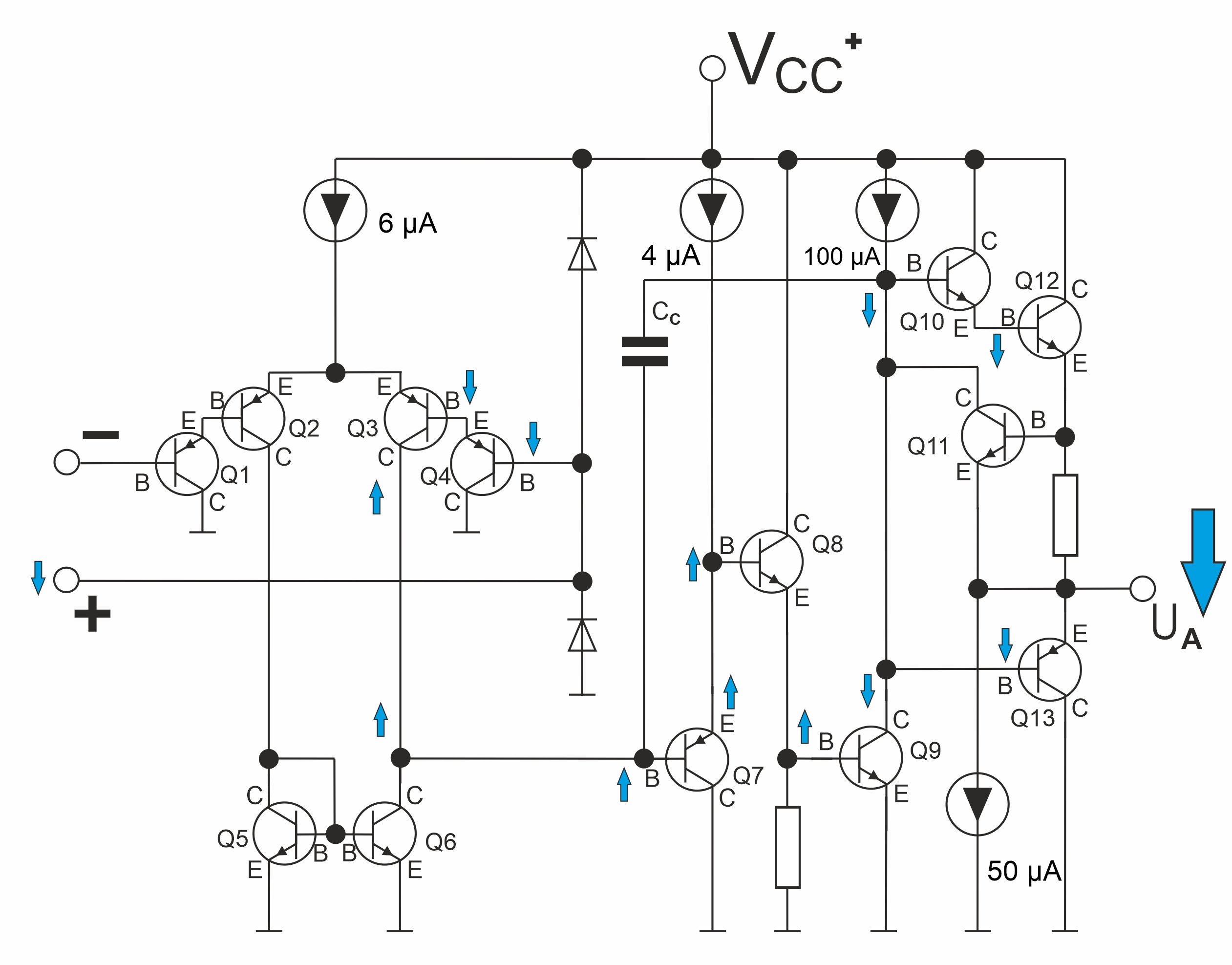
Negative voltage change at the non-inverted input (+)
A negative voltage change at the non-inverting input causes transistor Q4 to conduct more strongly. This reduces the voltage at the base of transistor Q3, causing Q3 to conduct more strongly as well. The voltage at the collector of Q3 and thus also at the base of Q7 increases.
Transistor Q7 becomes more high-impedance, causing the voltage at the emitter of Q7 to rise. Because transistor Q8 now receives a higher base voltage, it conducts more.
The voltage at the emitter of Q8 and at the base of Q9 rises. Transistor Q9 conducts more and the voltage at the collector of Q9 and at the base of Q13 drops.
Transistor Q13 becomes low-impedance and pulls the output to the negative potential of the operating voltage.
At the same time, the collector/emitter paths of transistors Q10 and Q12 become more high-impedance or block.
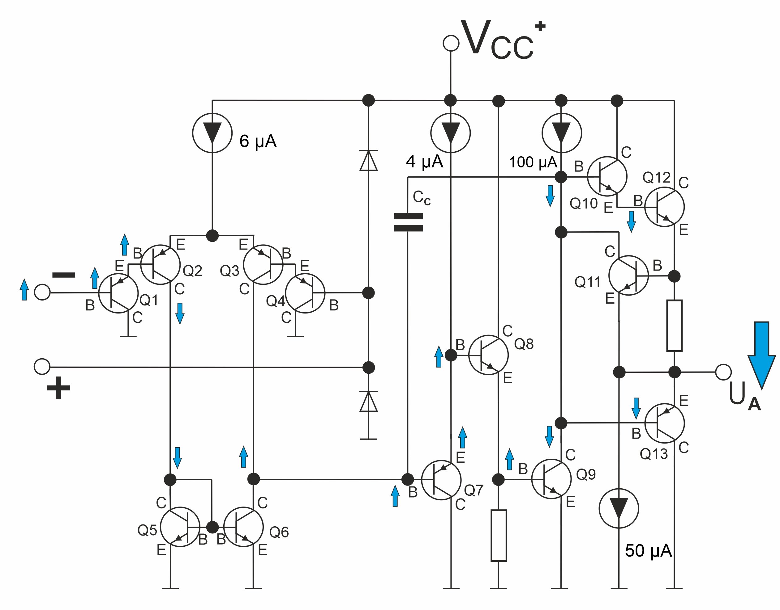
Positive voltage change at the inverted input (-)
When the voltage at the inverted input rises, the collector/emitter path of Q1 becomes more high-impedance. This causes the voltage at the emitter of Q1 or at the base of Q2 to rise. As a result, Q2 also becomes more high-impedance and the voltage at the collector of Q2 decreases. Due to the now higher resistance of Q2, the current flow through transistors Q2 and Q5 decreases.
The two transistors Q5 and Q6 function as current mirrors. This means that the collector/emitter current through transistor Q6 is always exactly the same as the current through the collector/emitter path of Q5.
The decreasing collector voltage of Q5 is also present at the base of transistors Q5 and Q6. Due to the reduced base voltage, Q6 blocks more strongly, causing the current to drop and the collector voltage to rise. This causes the current through Q6 to be equalized with the current through Q5. The further signal progression corresponds to the negative voltage change at the non-inverted input (+).
This means that a voltage increase at the inverted input results in a voltage decrease at the output.
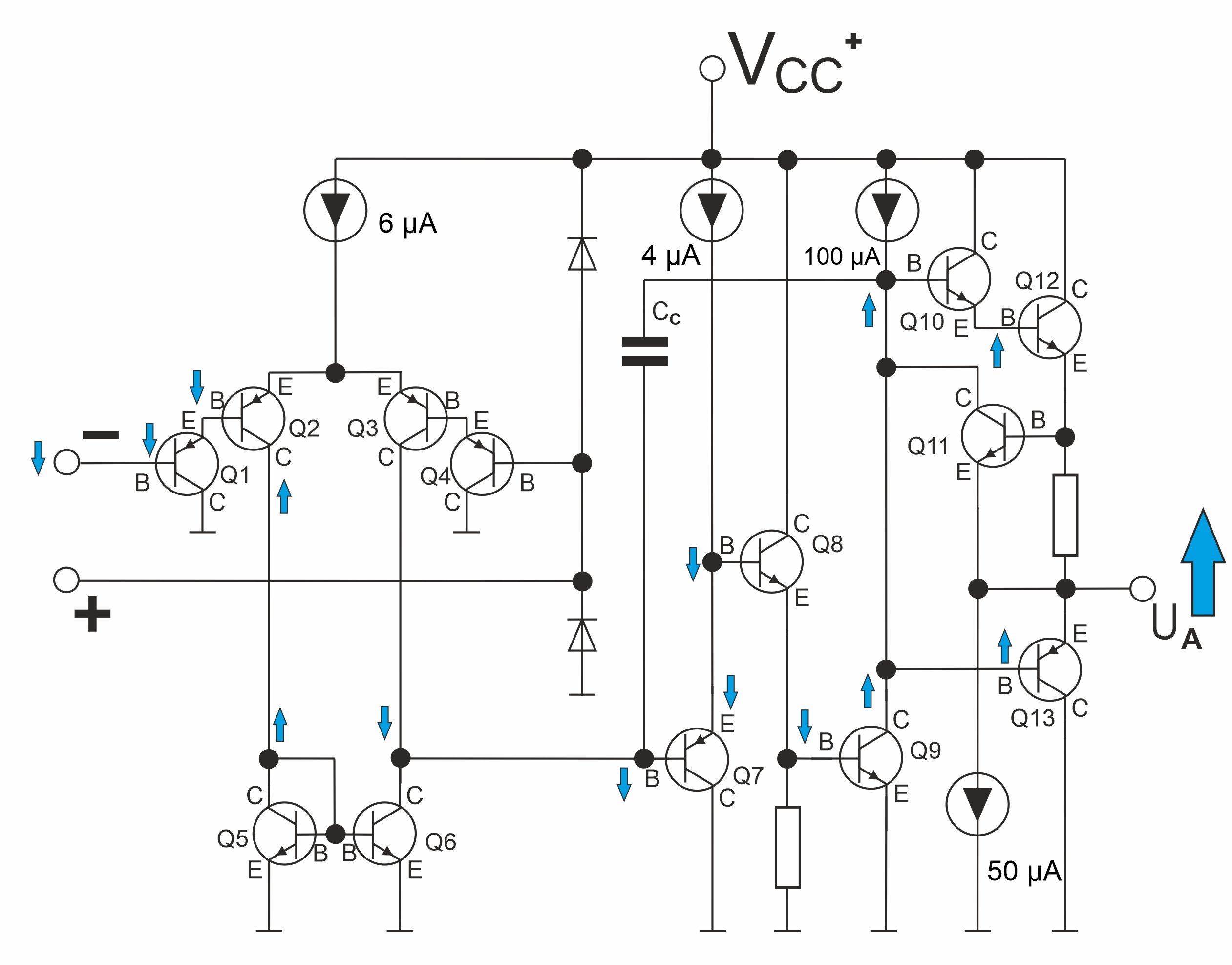
Negative voltage change at the inverted input (-)
A negative voltage change at the inverting input causes transistor Q1 to conduct more strongly. This reduces the voltage at the base of transistor Q2, causing Q2 to conduct more strongly as well.
The voltage at the collector of transistor Q2 and at the collector of transistor Q5 increases. The current flow through transistors Q2 and Q5 becomes higher.
The higher collector voltage of Q5 is transmitted to the base of transistors Q5 and Q6, causing Q6 to conduct more strongly. The collector current increases and the collector voltage decreases. The current through Q6 is thus also adjusted to the current through Q5 in this case.
The further signal progression corresponds to the positive voltage change at the non-inverted input (+).
This means that a voltage drop at the inverted input results in a voltage increase at the output.
According to the manufacturer, the IC LM324 is primarily intended for use in electronics as well as for use in control and regulation technology.
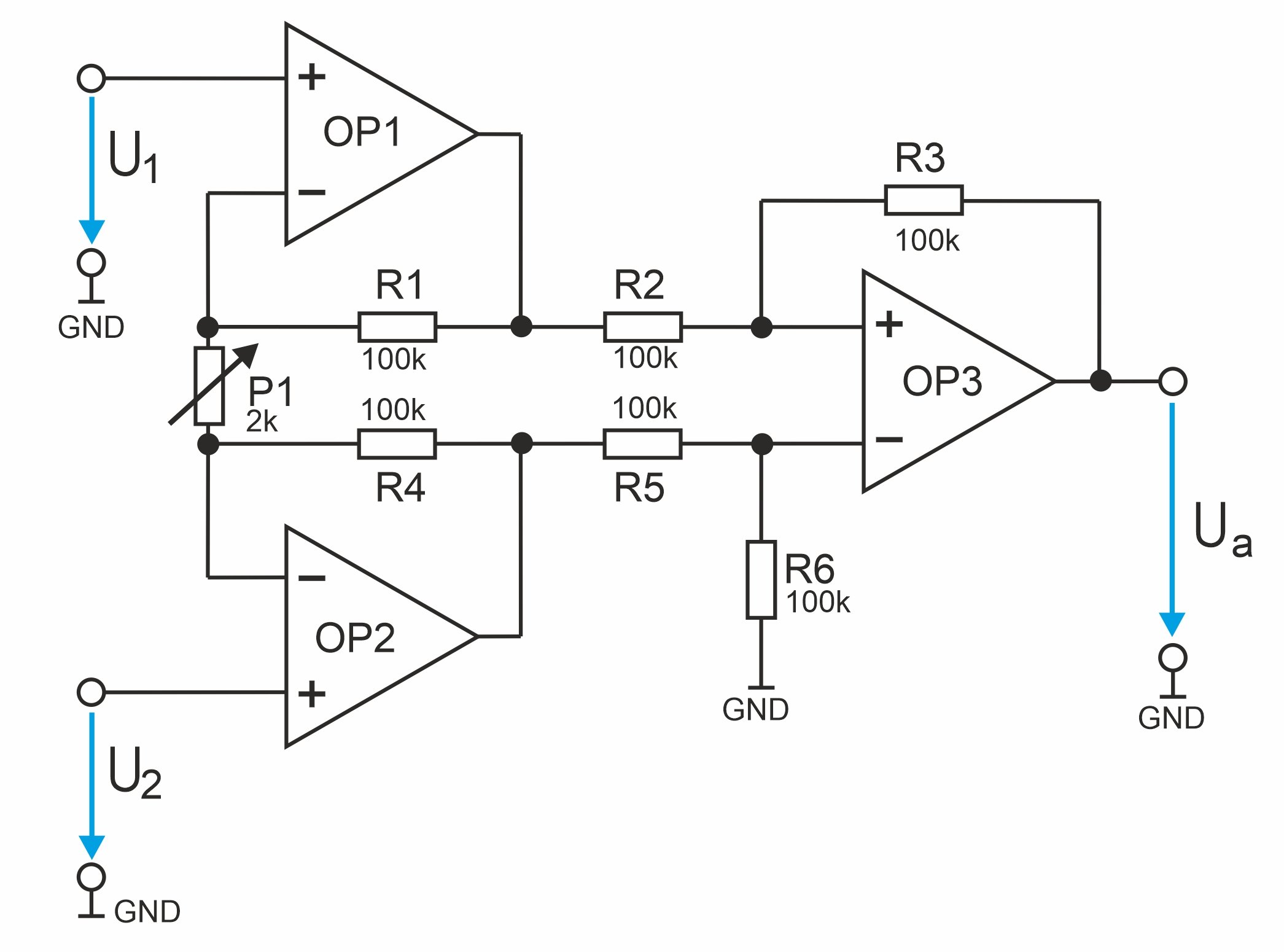
However, it can also be used for a wide variety of OPV applications. The manufacturer has listed several circuit examples for amplifiers and filters in the data sheet, whereby the instrument amplifier circuit or the instrumentation amplifier circuit with three OPVs should be examined in more detail.
Instrument amplifiers are needed because accelerometers, force sensors, strain gauges, and pressure transducers deliver weak differential signals. The signals from these sensors must be recorded and amplified for further evaluation.
The two operational amplifiers OP1 and OP2 operate as negative feedback amplifier stages. The third OP amplifier operates as a subtractor, which performs common-mode rejection. Common-mode rejection prevents a change in the output voltage when the voltages at the two inputs of an OPV change by the same amount (common mode) at the same time.
